In essence, sputtering is a physical process used to create ultra-thin films of material on a surface. It works by bombarding a source material, called a "target," with energized ions inside a vacuum chamber. This atomic-scale bombardment physically knocks off, or "sputters," atoms from the target, which then travel and deposit onto a nearby object, called the "substrate," forming the desired thin film.
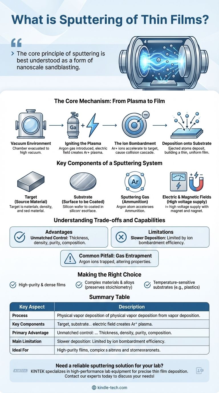
The core principle of sputtering is best understood as a form of nanoscale sandblasting. Instead of sand, it uses ionized gas particles to precisely chip away atoms from a source material, which then recoat another surface with exceptional control over the final film's properties.
The Core Mechanism: From Plasma to Film
To understand sputtering, it's best to break the process down into its fundamental stages, which all occur within a controlled vacuum environment.
The Vacuum Environment
First, both the target (the source material) and the substrate (the surface to be coated) are placed inside a high-vacuum chamber. This vacuum is critical because it removes other gas molecules that could contaminate the film or interfere with the process.
Igniting the Plasma
A small, controlled amount of an inert gas, almost always Argon, is introduced into the chamber. An electric field is then applied, which strips electrons from the Argon atoms. This creates a glowing, energized state of matter called a plasma, consisting of positive Argon ions (Ar+) and free electrons.
The Ion Bombardment
The target material is given a strong negative electrical charge, making it a cathode. The positively charged Argon ions in the plasma are naturally and powerfully accelerated toward this negatively charged target.
These ions strike the target surface with significant kinetic energy. This impact sets off a series of atomic-scale collisions within the target material, known as a collision cascade.
Deposition onto the Substrate
When these collision cascades reach the surface of the target, they transfer enough energy to eject individual target atoms. These sputtered atoms travel through the vacuum chamber and land on the substrate.
Over time, these atoms build up layer by layer, forming a thin, uniform, and highly controlled film on the substrate's surface.
Key Components of a Sputtering System
While systems vary, they all rely on the same fundamental components to function.
The Target (Source Material)
This is a block or plate made of the material you wish to deposit as a thin film. Sputtering can be used with a vast range of materials, including pure metals, alloys, and ceramic compounds.
The Substrate (The Surface to be Coated)
This is the object that receives the coating. Substrates can be anything from silicon wafers and glass panels to molded plastics and medical implants.
The Sputtering Gas (The "Ammunition")
Argon is the standard choice because it is chemically inert, preventing unwanted reactions, and has a high atomic weight, making it effective at dislodging target atoms upon impact.
The Role of Electric and Magnetic Fields
A high-voltage power supply creates the crucial electric field that accelerates the ions. Many modern systems also use powerful magnets behind the target in a configuration known as magnetron sputtering. These magnets trap electrons near the target, dramatically increasing the efficiency of the gas ionization and leading to much faster deposition rates.
Understanding the Trade-offs and Capabilities
Sputtering is a powerful technique, but like any process, it involves specific advantages and limitations that make it suitable for certain applications over others.
The Primary Advantage: Unmatched Control
Sputtering offers exceptionally precise control over a film's thickness, density, purity, and composition. Because the target material is transferred atom by atom without being melted, even complex alloys and compounds can be deposited while preserving their original chemical ratios.
The Main Limitation: Slower Deposition
Compared to thermal processes like evaporation, where a material is simply boiled off, sputtering is often a slower deposition method. The rate of material transfer is limited by the efficiency of the ion bombardment.
Common Pitfall: Gas Entrapment
In some cases, the Argon ions used for sputtering can become embedded or trapped within the growing thin film. While often a minor issue, this can alter the film's properties and must be managed for high-purity applications.
Making the Right Choice for Your Goal
Sputtering is chosen when the precision and quality of the thin film are more important than the speed of deposition.
- If your primary focus is high-purity and dense films: Sputtering excels because the process transfers the target material's composition with high fidelity and the energetic deposition creates tightly packed film structures.
- If your primary focus is coating with complex materials or alloys: Sputtering is ideal as it doesn't require melting the source material, preserving the original stoichiometry (chemical ratio) of the compound.
- If your primary focus is coating temperature-sensitive substrates (like plastics): Sputtering is a relatively low-temperature process, making it a superior choice for depositing high-performance films onto materials that cannot withstand significant heat.
Ultimately, sputtering is a cornerstone of modern manufacturing, enabling the precise engineering of surfaces for everything from semiconductor chips to advanced optical lenses.
Summary Table:
| Key Aspect | Description |
|---|---|
| Process | Physical vapor deposition via ion bombardment in a vacuum. |
| Key Components | Target (source material), substrate (coated surface), Argon gas, electric/magnetic fields. |
| Primary Advantage | Unmatched control over film thickness, density, purity, and composition. |
| Main Limitation | Slower deposition rate compared to thermal processes like evaporation. |
| Ideal For | High-purity films, complex alloys, temperature-sensitive substrates (e.g., plastics). |
Need a reliable sputtering solution for your lab? KINTEK specializes in high-performance lab equipment and consumables for precise thin film deposition. Whether you're working with semiconductors, optics, or advanced materials, our sputtering systems deliver the control and purity your research demands. Contact our experts today to discuss how we can support your laboratory's specific needs!
Visual Guide
Related Products
- Spark Plasma Sintering Furnace SPS Furnace
- Vacuum Induction Melting Spinning System Arc Melting Furnace
- Chemical Vapor Deposition CVD Equipment System Chamber Slide PECVD Tube Furnace with Liquid Gasifier PECVD Machine
- Customer Made Versatile CVD Tube Furnace Chemical Vapor Deposition Chamber System Equipment
People Also Ask
- What are the advantages of CAMI/SPS for W-Cu composite preparation? Reduce cycles from hours to seconds.
- What is the mechanism of SPS process? A Deep Dive into Rapid, Low-Temperature Sintering
- What is SPS sintering method? A Guide to High-Speed, High-Performance Material Fabrication
- What is the difference between spark plasma sintering and flash sintering? A Guide to Advanced Sintering Methods
- What technical advantages does a Spark Plasma Sintering (SPS) furnace offer for LZP ceramics? Enhance Ionic Conductivity


