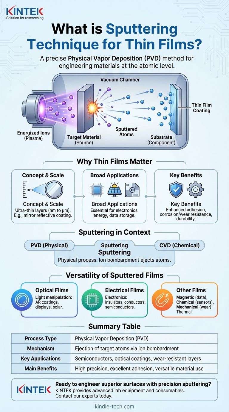
At its core, sputtering is a highly controlled method for depositing exceptionally thin layers of material onto a surface. It is a type of Physical Vapor Deposition (PVD) where atoms are ejected from a source material, known as a "target," and then deposited onto a component, called a "substrate," to form a new functional coating. This process is fundamental to manufacturing countless modern technologies, from microchips to advanced glass.
Sputtering is not merely a coating process; it is a technique for engineering materials at the atomic level. It allows us to imbue everyday objects with new properties—like conductivity, durability, or reflectivity—that are essential for high-performance applications.
Why Thin Films Matter
Before diving deeper into sputtering, it's crucial to understand what thin films are and why they are so indispensable across industries.
The Concept of a Thin Film
A thin film is a layer of material ranging from fractions of a nanometer to several micrometers in thickness. A household mirror provides a perfect example: a very thin layer of metal is applied to the back of a glass sheet, creating the reflective surface we use every day.
Broad Industrial Applications
The use of thin films is widespread and critical. They are used to create protective coatings, convert light into electricity in solar cells, and enable advanced data storage devices. Their versatility makes them a cornerstone of modern manufacturing.
Key Benefits of Thin Film Coatings
Applying a thin film can dramatically improve a material's properties. Key benefits include enhanced adhesion, superior corrosion and wear resistance, and increased durability. They can also provide aesthetic advantages, changing a substrate's color or making it more reflective.
Sputtering in the Context of Deposition
Sputtering is one of several methods used to create thin films. Understanding its place among other techniques clarifies its unique role.
The Two Major Deposition Families
Virtually all thin film deposition techniques fall into two main categories: Physical Vapor Deposition (PVD) and Chemical Vapor Deposition (CVD). Sputtering is one of the most common and versatile PVD methods.
How Sputtering Works
Sputtering is a physical process. It involves bombarding a target material with energized ions inside a vacuum. This impact physically ejects or "sputters" atoms from the target, which then travel and deposit onto the substrate, building the thin film one atom at a time.
The Versatility of Sputtered Films
The high degree of control offered by sputtering allows for the creation of many different types of films, each engineered for a specific function.
Optical and Electrical Films
The applications are incredibly diverse. Optical thin films are used for everything from anti-reflective coatings on eyeglasses to solar cells and digital monitors. Electrical thin films are fundamental to electronics, forming the insulators, conductors, and semiconductor devices inside integrated circuits.
Expanding the Scope
Beyond optics and electronics, sputtered films serve many other purposes. They include magnetic films for data storage, chemical films for sensors, mechanical films for wear resistance, and thermal films for insulation.
Understanding the Impact of This Technique
The specific type of thin film created determines its application. Sputtering is the enabling technology behind many of these specialized coatings.
- If your primary focus is manipulating light: Sputtering is used to create precise optical films for reflective coatings, lenses, solar panels, and displays.
- If your primary focus is electronics: This technique is essential for building the microscopic conductive and insulating layers required for semiconductor devices and integrated circuits.
- If your primary focus is material durability: Sputtered films provide robust coatings that protect components from corrosion, friction, and wear in demanding environments.
Ultimately, sputtering is a foundational process that allows us to precisely engineer the surfaces of materials, unlocking the performance required by our most advanced technologies.
Summary Table:
| Aspect | Key Detail |
|---|---|
| Process Type | Physical Vapor Deposition (PVD) |
| Primary Mechanism | Ejection of target atoms via ion bombardment |
| Key Applications | Semiconductor devices, optical coatings, wear-resistant layers |
| Main Benefits | High precision, excellent adhesion, versatile material use |
Ready to engineer superior surfaces with precision sputtering?
KINTEK specializes in providing advanced lab equipment and consumables for all your thin film deposition needs. Whether you are developing semiconductor devices, optical coatings, or durable protective layers, our solutions deliver the accuracy and reliability your research demands.
Contact our experts today to discuss how we can support your laboratory's specific projects and help you achieve breakthrough results.
Visual Guide
Related Products
- Spark Plasma Sintering Furnace SPS Furnace
- Vacuum Induction Melting Spinning System Arc Melting Furnace
- Chemical Vapor Deposition CVD Equipment System Chamber Slide PECVD Tube Furnace with Liquid Gasifier PECVD Machine
- Customer Made Versatile CVD Tube Furnace Chemical Vapor Deposition Chamber System Equipment
- Vacuum Cold Mounting Machine for Sample Preparation
People Also Ask
- Why are Spark Plasma Sintering (SPS) furnaces or hot presses utilized in the preparation of Li3PS4 solid electrolytes?
- What technical advantages does a Spark Plasma Sintering (SPS) furnace offer for LZP ceramics? Enhance Ionic Conductivity
- What is the pressure for spark plasma sintering? A Guide to Optimizing SPS Parameters
- What is the difference between spark plasma sintering and flash sintering? A Guide to Advanced Sintering Methods
- What are the advantages of CAMI/SPS for W-Cu composite preparation? Reduce cycles from hours to seconds.


