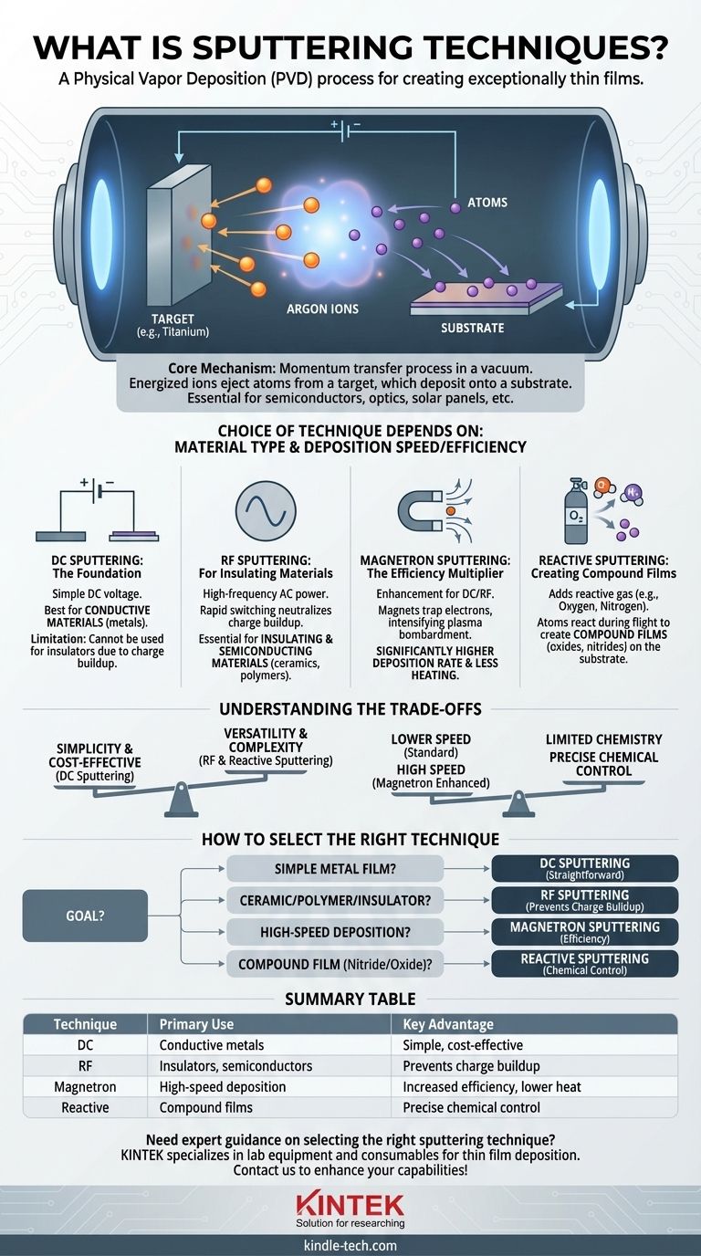
Sputtering is a physical vapor deposition (PVD) technique used to create exceptionally thin films of material on a surface, known as a substrate. The process takes place in a vacuum and involves bombarding a source material, or "target," with energized ions, which eject atoms from the target that then travel and deposit onto the substrate. This method is fundamental to manufacturing a wide range of modern products, from semiconductor chips and optical lenses to hard drives and solar panels.
While all sputtering involves ejecting atoms from a target to coat a substrate, the specific technique you choose is determined by two critical factors: the type of material you need to deposit and the deposition speed and efficiency your process requires.
The Core Mechanism: How Sputtering Works
At its heart, sputtering is a momentum transfer process, much like a cue ball striking a rack of billiard balls. Understanding the basic setup clarifies why different techniques are necessary.
The Vacuum Environment
All sputtering occurs in a vacuum chamber. This is critical to ensure the ejected target atoms can travel to the substrate without colliding with air molecules, which would contaminate the film and disrupt the process.
The Target and Substrate
The target is a block of the material you wish to deposit (e.g., titanium, silicon, gold). The substrate is the object you are coating (e.g., a silicon wafer, a piece of glass, a medical implant).
Plasma and Ion Bombardment
An inert gas, almost always argon, is introduced into the chamber at low pressure. An electric field is then applied, which strips electrons from the argon atoms, creating a glowing, ionized gas called a plasma. The positively charged argon ions are then accelerated into the negatively charged target, striking it with enough force to knock off, or "sputter," individual atoms.
Key Sputtering Techniques and Their Purpose
The differences between sputtering techniques arise from how the electric field is generated and whether other enhancements are used.
DC (Direct Current) Sputtering: The Foundation
DC sputtering is the simplest form. A high DC voltage is applied between the target (cathode) and the substrate (anode). This works exceptionally well for electrically conductive target materials, like most metals.
However, if you try to use DC sputtering on an insulating material, positive charge builds up on the target's surface, effectively repelling the incoming argon ions and shutting the process down.
RF (Radio Frequency) Sputtering: For Insulating Materials
To solve the charge buildup problem, RF sputtering uses a high-frequency alternating current (AC) power source instead of DC. The field rapidly switches between positive and negative.
This rapid switching allows it to sputter insulating and semiconducting materials like ceramics (e.g., silicon dioxide) or polymers. The alternating field effectively neutralizes the charge buildup on the target surface during each cycle, allowing the process to continue.
Magnetron Sputtering: The Efficiency Multiplier
Magnetron sputtering is not a standalone technique but rather a powerful enhancement to both DC and RF sputtering. It involves placing strong magnets behind the target.
These magnets trap electrons from the plasma in a magnetic field close to the target's surface. This dramatically increases the number of argon ions created in that region, leading to a much more intense bombardment of the target. The result is a significantly higher deposition rate and less heating of the substrate.
Reactive Sputtering: Creating Compound Films
Reactive sputtering is a process variation where a reactive gas, such as oxygen or nitrogen, is intentionally added to the argon in the vacuum chamber.
As atoms are sputtered from a primary target (e.g., titanium), they react with this gas on their way to the substrate. This allows for the creation of compound films, such as titanium nitride (a hard coating) or titanium dioxide (an optical coating), directly on the substrate.
Understanding the Trade-offs
Choosing a technique requires balancing material needs, process complexity, and desired outcomes.
Material Compatibility vs. Simplicity
DC sputtering is simple and cost-effective, but it is fundamentally limited to conductive targets. RF sputtering is far more versatile, handling virtually any material, but the equipment is more complex and expensive.
Deposition Rate vs. Process Control
Standard DC or RF sputtering (without a magnetron) is relatively slow. Adding a magnetron provides a major boost in deposition speed, making it ideal for industrial-scale production.
Film Chemistry vs. Simplicity
Reactive sputtering provides incredible control over the chemical composition of the final film. However, it adds significant complexity, as the flow rates of both the inert and reactive gases must be controlled with extreme precision to achieve the desired stoichiometry.
How to Select the Right Sputtering Technique
Your choice of sputtering technique should be driven directly by your project's goal.
- If your primary focus is depositing a simple metal film: DC sputtering is the most straightforward and cost-effective method.
- If your primary focus is depositing a ceramic, polymer, or other insulator: RF sputtering is essential to prevent electrical charge buildup on the target.
- If your primary focus is high-speed deposition or coating heat-sensitive substrates: Magnetron sputtering (combined with either DC or RF) is the superior choice for its efficiency and lower thermal load.
- If your primary focus is creating a specific compound film like a nitride or oxide: Reactive sputtering is the necessary technique to control the film's final chemical composition.
Understanding these core distinctions empowers you to select the precise sputtering method that aligns with your material, budget, and performance goals.
Summary Table:
| Technique | Primary Use | Key Advantage |
|---|---|---|
| DC Sputtering | Conductive metals | Simple, cost-effective |
| RF Sputtering | Insulators, semiconductors | Prevents charge buildup |
| Magnetron Sputtering | High-speed deposition | Increased efficiency, lower heat |
| Reactive Sputtering | Compound films (nitrides, oxides) | Precise chemical control |
Need expert guidance on selecting the right sputtering technique for your lab? KINTEK specializes in lab equipment and consumables, providing tailored solutions for your thin film deposition needs. Whether you're working with semiconductors, optical coatings, or solar panels, our expertise ensures optimal process efficiency and material performance. Contact us today to discuss how we can enhance your laboratory capabilities!
Visual Guide