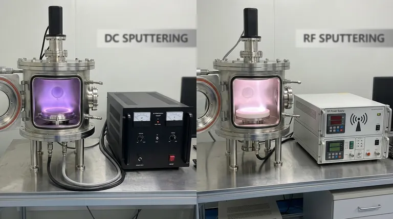
The fundamental difference between RF and DC sputtering lies in the power source, which in turn dictates the type of material you can deposit. DC (Direct Current) sputtering uses a static charge and is highly effective for conductive materials like metals. RF (Radio Frequency) sputtering uses an alternating current, which prevents charge buildup on the target surface, making it the essential choice for depositing non-conductive, insulating materials.
Your choice between RF and DC sputtering is not about which method is superior overall, but which is correct for your specific target material. DC sputtering is a fast, economical workhorse for conductive targets, while RF sputtering provides the critical versatility to deposit insulating films.
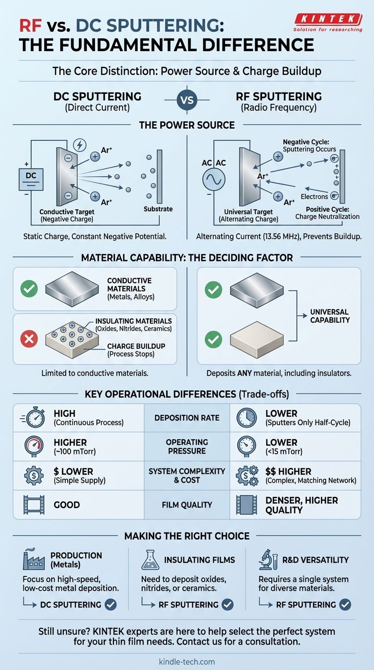
The Core Distinction: Power Source and Charge Buildup
The choice of power source creates a critical difference in how each sputtering process functions at the atomic level. This difference is entirely about managing electrical charge on the surface of the target material.
How DC Sputtering Works (And Its Limitation)
In DC sputtering, a high DC voltage is applied to the target, giving it a constant negative charge. This negatively charged target attracts positively charged ions from the gas plasma (typically Argon).
These ions accelerate and collide with the target, physically knocking off atoms that then travel and deposit onto your substrate. This process is simple and efficient, but it relies on one key assumption: the target must be electrically conductive to dissipate the positive charge from the arriving ions and maintain the negative potential.
If you use an insulating (dielectric) target, positive ions accumulate on the surface. This is called charge buildup. This positive layer quickly repels incoming positive ions, effectively stopping the sputtering process entirely.
How RF Sputtering Solves the Problem
RF sputtering replaces the DC power supply with an AC source operating at radio frequencies (typically 13.56 MHz). This rapidly alternates the target's charge between positive and negative.
During the negative half-cycle, the target attracts positive ions, and sputtering occurs just as it does in the DC process.
During the brief positive half-cycle, the target attracts electrons from the plasma. These electrons flood the surface and neutralize the excess positive charge that built up during the sputtering portion of the cycle. This action acts as a self-cleaning mechanism, preventing charge buildup and allowing the process to continue indefinitely, regardless of the target material's conductivity.
Key Operational Differences
The choice of power supply leads to several practical consequences in terms of performance, cost, and the quality of the resulting thin film.
Material Capability: The Deciding Factor
This is the most important difference.
- DC Sputtering: Limited to conductive materials like pure metals and conductive alloys.
- RF Sputtering: Universal. It can be used for any material, including conductors, but its unique advantage is the ability to deposit insulators like oxides (SiO₂), nitrides (Si₃N₄), and ceramics.
Deposition Rate and Efficiency
Because sputtering only occurs during the negative portion of the AC cycle, RF sputtering generally has a lower deposition rate than DC sputtering. DC sputtering is a continuous, uninterrupted process, making it faster and more efficient for depositing conductive films.
Operating Pressure
RF power is more efficient at sustaining a plasma. This allows RF systems to operate at lower gas pressures (e.g., under 15 mTorr) compared to DC systems (which may require up to 100 mTorr).
Operating at lower pressures reduces the chance that sputtered atoms will collide with gas atoms on their way to the substrate. This more direct path can result in a denser, higher-quality film.
System Complexity and Cost
DC power supplies are relatively simple and inexpensive. RF systems are more complex, requiring an RF power supply and an impedance matching network to efficiently transfer power to the plasma. This makes RF sputtering systems more expensive to purchase and maintain.
Understanding the Trade-offs
Neither method is perfect; each comes with clear trade-offs tied directly to its operating principle.
The Cost of Versatility (RF)
The primary benefit of RF sputtering is its ability to deposit any material. However, this versatility comes at a price:
- Slower deposition rates.
- Higher equipment cost.
- Increased system complexity.
The Limits of Simplicity (DC)
DC sputtering is valued for its speed, simplicity, and cost-effectiveness. The trade-off is its profound limitation:
- Strictly for conductive targets.
- Attempting to use it for insulators will fail due to charge buildup.
Making the Right Choice for Your Application
Your decision should be guided by the material you need to deposit and your operational priorities.
- If your primary focus is depositing conductive materials (like pure metals) at high speed and low cost: DC sputtering is the clear and optimal choice for production environments.
- If your primary focus is depositing insulating or dielectric materials (like oxides, nitrides, or ceramics): RF sputtering is the necessary and correct tool for the job.
- If you need a single, versatile system for research and development involving both material types: An RF sputtering system provides the essential flexibility you need, despite its higher initial cost and lower deposition rates.
Ultimately, understanding this fundamental difference in charge management empowers you to select the right tool based on the physics of your material.
Summary Table:
| Feature | DC Sputtering | RF Sputtering |
|---|---|---|
| Power Source | Direct Current (DC) | Radio Frequency (AC) |
| Target Material | Conductive materials (metals) | All materials (conductors & insulators) |
| Charge Buildup | Occurs with insulators, stops process | Neutralized by AC cycle, no buildup |
| Deposition Rate | High | Lower |
| Operating Pressure | Higher (~100 mTorr) | Lower (<15 mTorr) |
| Film Quality | Good | Denser, higher quality |
| System Cost | Lower | Higher |
| Best For | Fast, economical metal deposition | Versatile deposition of oxides, nitrides, ceramics |
Still unsure which sputtering method is right for your project? The experts at KINTEK are here to help. We specialize in providing lab equipment and consumables for all your thin film deposition needs. Whether you're working with conductive metals or complex insulating ceramics, we can help you select the perfect system to achieve high-quality, reliable results.
Contact our team today for a personalized consultation and discover how KINTEK can support your laboratory's success.
Visual Guide
Related Products
- Spark Plasma Sintering Furnace SPS Furnace
- Vacuum Induction Melting Spinning System Arc Melting Furnace
- Chemical Vapor Deposition CVD Equipment System Chamber Slide PECVD Tube Furnace with Liquid Gasifier PECVD Machine
- Customer Made Versatile CVD Tube Furnace Chemical Vapor Deposition Chamber System Equipment
People Also Ask
- What is the pressure for spark plasma sintering? A Guide to Optimizing SPS Parameters
- What are the advantages of CAMI/SPS for W-Cu composite preparation? Reduce cycles from hours to seconds.
- Why are Spark Plasma Sintering (SPS) furnaces or hot presses utilized in the preparation of Li3PS4 solid electrolytes?
- What is the process fundamentals of spark plasma sintering? Achieve Rapid, High-Density Material Consolidation
- What is SPS sintering method? A Guide to High-Speed, High-Performance Material Fabrication


