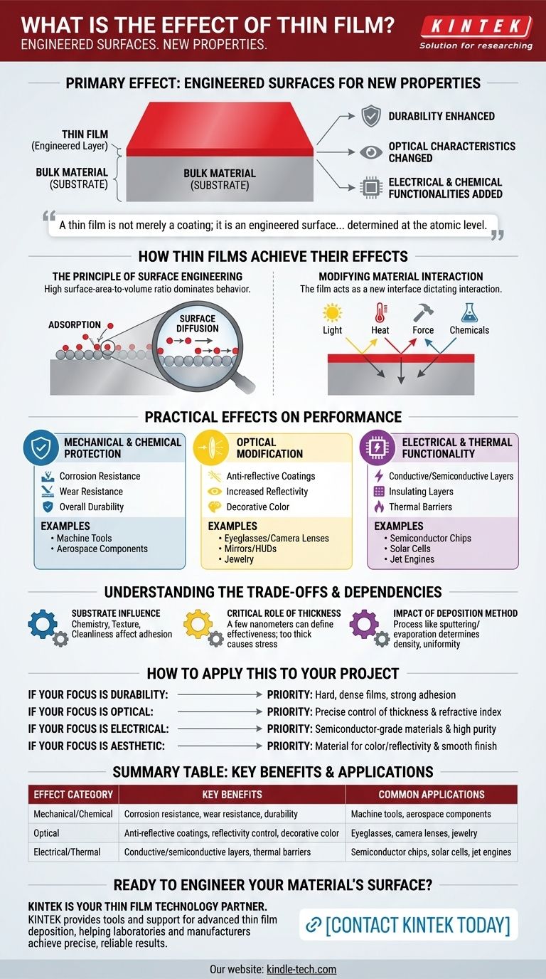
The primary effect of a thin film is to impart entirely new properties to the surface of a material without changing its core structure. By applying a layer that can be as thin as a few atoms, you can fundamentally alter a material's interaction with its environment, enhancing its durability, changing its optical characteristics, or adding new electrical and chemical functionalities.
A thin film is not merely a coating; it is an engineered surface. Its effect is to create a composite material where the bulk properties of the substrate are preserved, while the surface is given powerful new capabilities determined at the atomic level.
How Thin Films Achieve Their Effects
A thin film's power comes from its high surface-area-to-volume ratio. At this scale, the physics of surfaces, rather than the bulk material properties, dominate its behavior.
The Principle of Surface Engineering
Materials reduced to the scale of a thin film behave differently than their bulk counterparts. The vast majority of the film's atoms are either on the surface or very close to it.
This proximity to the surface means that properties like adsorption (atoms sticking to the surface) and surface diffusion (atoms moving across the surface) become the defining characteristics of the material's behavior.
Modifying Material Interaction
The film acts as a new interface between the original material (the substrate) and the outside world. This new interface dictates how the object interacts with light, heat, physical force, and chemical agents.
The Practical Effects on Performance
The theoretical principles of surface engineering translate into tangible, highly valuable effects across multiple categories.
Mechanical and Chemical Protection
One of the most common effects is enhanced protection. The film acts as a barrier, shielding the substrate from environmental harm.
This leads to dramatic improvements in corrosion resistance, wear resistance, and overall durability, which is why thin films are used for protective coatings on everything from machine tools to aerospace components.
Optical Modification
Thin films can precisely control how light interacts with a surface. A single layer or multiple layers can be engineered to achieve specific outcomes.
This includes creating anti-reflective coatings for eyeglasses and camera lenses, increasing reflectivity for mirrors and head-up displays, or adding decorative color to jewelry.
Electrical and Thermal Functionality
Thin films are the foundation of modern electronics. By depositing specific materials, you can create the conductive, semiconductive, and insulating layers essential for devices.
This effect is critical in manufacturing semiconductor chips, solar cells, touch-panel screens, and even thin-film batteries. They can also act as thermal barriers in high-temperature applications like jet engines.
Understanding the Trade-offs and Dependencies
The effect of a thin film is not guaranteed; it is the result of a highly controlled process where several factors must be managed. Achieving the desired outcome depends on a sensitive balance.
The Influence of the Substrate
The underlying material is not just a passive carrier. The film's ability to adhere and form a proper structure is directly influenced by the substrate's chemistry, texture, and cleanliness. Poor substrate preparation can lead to film failure.
The Critical Role of Thickness
Film thickness is a primary variable. A few nanometers can mean the difference between an effective anti-reflection coating and one that doesn't work. Thicker films may offer more durability but can also introduce internal stresses that cause cracking or delamination.
The Impact of the Deposition Method
How the film is applied—whether through sputtering, evaporation, or chemical vapor deposition—has a profound impact on its final density, uniformity, and internal structure. The chosen method must align with the material being used and the desired effect.
How to Apply This to Your Project
Your choice of thin film technology should be guided entirely by the primary effect you need to achieve.
- If your primary focus is durability: Prioritize materials and deposition methods known for creating hard, dense films with strong adhesion to protect against wear and corrosion.
- If your primary focus is optical performance: Your design will revolve around precise control of film thickness and refractive index, often requiring multiple, highly uniform layers.
- If your primary focus is electrical function: You will need to use semiconductor-grade materials and high-purity deposition processes to create reliable conductive or insulating pathways.
- If your primary focus is aesthetic appeal: The key factors will be material choice for color and reflectivity, as well as a deposition process that ensures a smooth, uniform finish.
By understanding that a thin film is an engineered surface, you can select the right combination of material, thickness, and process to achieve your specific goal.
Summary Table:
| Effect Category | Key Benefits | Common Applications |
|---|---|---|
| Mechanical/Chemical | Corrosion resistance, wear resistance, durability | Machine tools, aerospace components |
| Optical | Anti-reflective coatings, reflectivity control, decorative color | Eyeglasses, camera lenses, jewelry |
| Electrical/Thermal | Conductive/semiconductive layers, thermal barriers | Semiconductor chips, solar cells, jet engines |
Ready to Engineer Your Material's Surface?
Thin film technology can unlock new levels of performance for your products. Whether you need enhanced durability, precise optical control, or specialized electrical functionality, KINTEK has the expertise and equipment to deliver.
As a specialist in lab equipment and consumables, we provide the tools and support necessary for advanced thin film deposition. Our solutions help laboratories and manufacturers achieve precise, reliable results.
Contact KINTEK today to discuss how thin film coatings can transform your materials and give you a competitive edge.
Visual Guide
Related Products
- Aluminum-Plastic Flexible Packaging Film for Lithium Battery Packaging
- Thin-Layer Spectral Electrolysis Electrochemical Cell
People Also Ask
- How to tell if a lithium-ion battery is bad? Spot the critical signs of failure before it's too late.
- What is the thinnest coating? Unlocking Unique Properties at the Atomic Scale
- What are the three types of lamination? Choose the Perfect Finish for Your Print Project
- Is there a way to test lithium batteries? Understand Voltage vs. True Health
- What are the properties of Aluminium (Al) relevant to its use in coatings? High Reflectivity & Conductivity Explored

