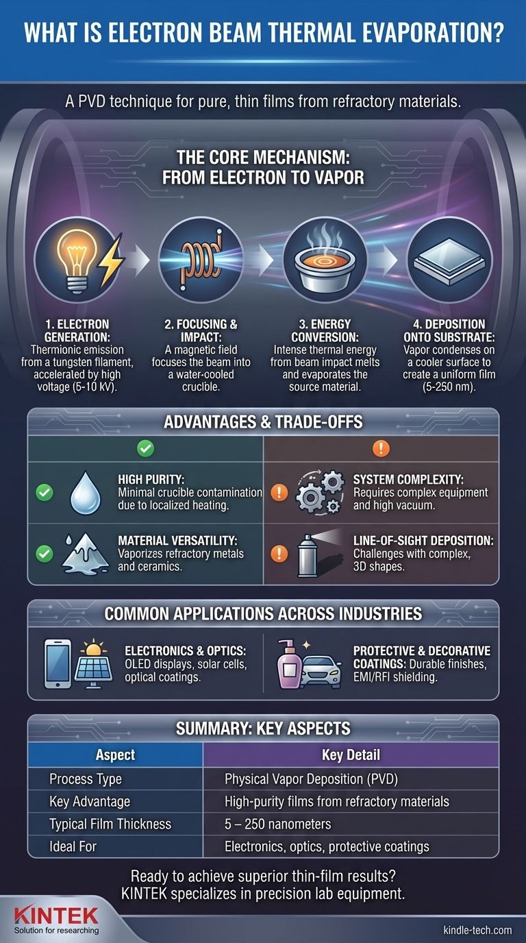
Electron beam thermal evaporation is a physical vapor deposition (PVD) technique that uses a focused, high-energy beam of electrons inside a vacuum to vaporize a source material. This vapor then travels and condenses onto a cooler surface, or substrate, creating an exceptionally thin and pure film. The intense, localized heating makes it possible to evaporate materials with very high melting points that are inaccessible to other methods.
At its core, electron beam evaporation is a method of converting the kinetic energy of accelerated electrons into intense thermal energy. This process offers precise control for creating high-purity, nanometer-scale coatings from a vast range of materials.
The Core Mechanism: From Electron to Vapor
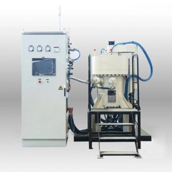
Electron beam evaporation is a multi-step process that takes place entirely within a high-vacuum chamber. This vacuum environment is critical, as it ensures the evaporated particles can travel to the substrate without colliding with air molecules or contaminants.
Generating the Electron Beam
The process begins with a tungsten filament, which is heated by a strong electric current. This intense heat causes thermionic emission, the release of electrons from the filament's surface. A high voltage, typically between 5 and 10 kilovolts (kV), is then applied to accelerate these free electrons toward the source material.
Focusing and Impact
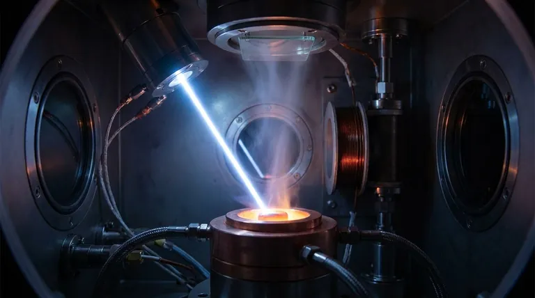
A magnetic field is used to precisely focus the accelerated electrons into a narrow beam. This beam is directed downward into a water-cooled copper crucible containing the material to be deposited, often called the target or source.
The Energy Conversion
When the high-energy electron beam strikes the target material, its kinetic energy is instantly converted into intense thermal energy. This rapid and concentrated heating causes the source material to melt and then evaporate (or sublimate, if it goes directly from solid to gas).
Deposition onto the Substrate
The evaporated material travels in a gaseous phase upwards from the crucible. It eventually reaches and condenses on the substrate, which is strategically positioned above the source. This condensation process builds a thin, uniform, and highly pure film on the substrate's surface, typically between 5 and 250 nanometers thick.
Understanding the Advantages and Trade-offs
While powerful, this technique has specific characteristics that make it ideal for certain applications and less suitable for others. Understanding these factors is key to leveraging its full potential.
The Advantage of High Purity
Because the electron beam heats only the surface of the source material, the crucible itself remains cool thanks to its water-cooling system. This prevents the crucible from melting or outgassing, which significantly reduces contamination and results in films of very high purity.
The Advantage of Material Versatility
The immense energy density of the electron beam can melt and vaporize virtually any material, including refractory metals and ceramics with extremely high melting points (e.g., tungsten, tantalum, titanium dioxide). This capability is a significant advantage over simpler thermal methods.
The Consideration of System Complexity
The equipment required—including a high-voltage power supply, magnetic focusing coils, an electron gun, and a high-vacuum system—is inherently more complex and costly than simpler deposition techniques like resistive thermal evaporation.
The Limitation of Line-of-Sight Deposition
Like a spray paint can, the vapor travels in a straight line from the source to the substrate. This "line-of-sight" characteristic means it is excellent for coating flat surfaces but can struggle to uniformly coat complex, three-dimensional objects with shadowed areas.
Common Applications Across Industries
The unique capabilities of e-beam evaporation make it a foundational process in the manufacturing of many advanced products.
Electronics and Optics
The technique is widely used to create thin-film devices like OLED displays and solar cells. It is also essential for manufacturing high-performance optical coatings, such as light reflectors for automotive headlamps, medical instruments, and aerospace components.
Protective and Decorative Coatings
E-beam evaporation is employed for applying durable and aesthetically pleasing finishes on consumer products like cosmetic closures and sporting goods. It is also used to deposit conductive layers for EMI/RFI shielding, which protects sensitive electronics from electromagnetic interference.
Making the Right Choice for Your Goal
Selecting a deposition method depends entirely on the material requirements and desired outcome of the film.
- If your primary focus is high-purity films or refractory materials: E-beam evaporation is the superior choice due to its direct, intense heating that avoids crucible contamination.
- If your primary focus is creating precise optical layers or electronic circuits: The control over deposition rate and material purity offered by this method is critical for achieving high performance.
- If your primary focus is coating simple shapes with low-melting-point materials: A less complex technique like resistive thermal evaporation might be a more cost-effective solution.
Ultimately, electron beam evaporation offers unparalleled control and versatility for creating advanced thin-film coatings from a vast library of materials.
Summary Table:
| Aspect | Key Detail |
|---|---|
| Process Type | Physical Vapor Deposition (PVD) |
| Key Advantage | High-purity films from refractory materials |
| Typical Film Thickness | 5 - 250 nanometers |
| Ideal For | Electronics, optics, protective coatings |
Ready to achieve superior thin-film results for your lab? KINTEK specializes in precision lab equipment and consumables for advanced deposition techniques like electron beam evaporation. Our solutions help laboratories working with electronics, optics, and high-performance coatings achieve exceptional purity and control. Contact our experts today to discuss how we can support your specific application needs.
Visual Guide
Related Products
- Molybdenum Tungsten Tantalum Evaporation Boat for High Temperature Applications
- RF PECVD System Radio Frequency Plasma-Enhanced Chemical Vapor Deposition RF PECVD
- Electron Beam Evaporation Coating Conductive Boron Nitride Crucible BN Crucible
- Hemispherical Bottom Tungsten Molybdenum Evaporation Boat
- E Beam Crucibles Electron Gun Beam Crucible for Evaporation
People Also Ask
- What is vacuum thermal evaporation? A Guide to High-Purity Thin Film Deposition
- What is the thermal evaporation technique? A Guide to Thin-Film Deposition for Your Lab
- What is the difference between sputtering and thermal evaporation? Choose the Right PVD Method for Your Thin Film
- What is thermal evaporation used to deposit? A Guide to Metals, Compounds, and Key Applications
- What is the meaning of thermal evaporation? A Guide to Simple, Cost-Effective Thin Film Coating