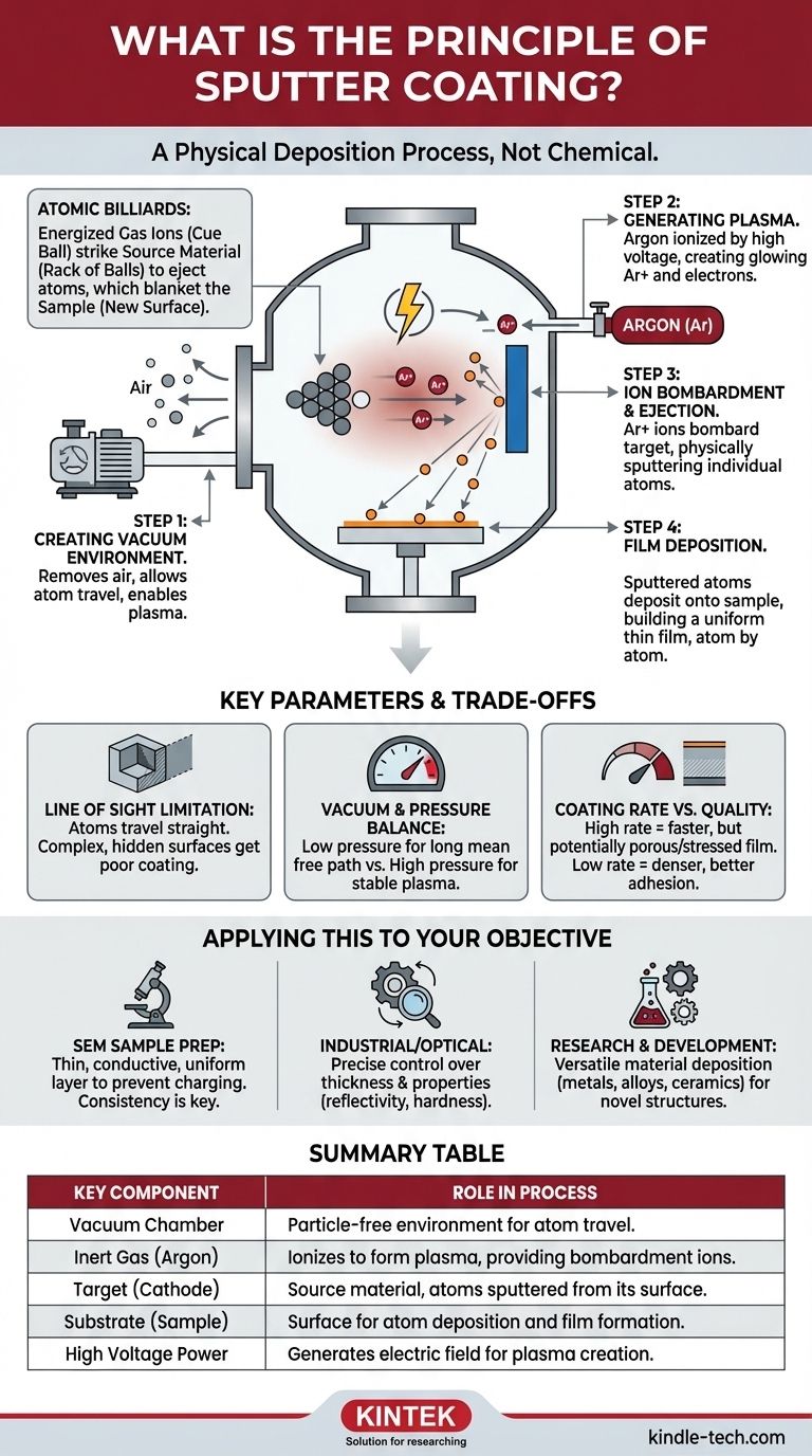
At its core, sputter coating is a physical deposition process, not a chemical one. Inside a vacuum chamber, high-energy ions, typically from an inert gas like argon, are accelerated into a source material called a "target." This bombardment acts like a microscopic sandblaster, physically ejecting or "sputtering" individual atoms from the target, which then travel and deposit onto a nearby sample, forming an exceptionally thin and uniform film.
Think of sputter coating not as a chemical reaction, but as a microscopic game of atomic billiards. By firing energized gas ions (the cue ball) at a source material (the rack of balls), you are physically knocking atoms loose, which then blanket your sample to form a new surface.
The Mechanics of Sputter Deposition
To understand why sputter coating is so widely used, from preparing samples for electron microscopes to manufacturing microchips, we must break down the process into its essential physical steps.
Step 1: Creating the Vacuum Environment
The entire process must occur in a vacuum. This is non-negotiable for two critical reasons.
First, it removes air and other particles that would otherwise collide with and scatter the sputtered atoms, preventing them from reaching the sample (the "substrate"). Second, a low-pressure environment is required to generate and sustain the plasma needed for the next step.
Step 2: Generating the Plasma
Once a vacuum is established, a small, precisely controlled amount of an inert gas, most commonly argon (Ar), is introduced into the chamber.
A high voltage is then applied, with the target material acting as the negative electrode (the cathode). This powerful electric field strips electrons from the argon atoms, creating a glowing, ionized gas known as a plasma, which consists of positive argon ions (Ar+) and free electrons.
Step 3: Ion Bombardment and Target Ejection
The positively charged argon ions (Ar+) are strongly attracted to and accelerate rapidly towards the negatively charged target.
Upon impact, the ions transfer their kinetic energy to the target material. If this energy is sufficient, it overcomes the forces binding the target's atoms together, causing them to be physically ejected or "sputtered" away from the surface.
Step 4: Film Deposition on the Substrate
The ejected atoms from the target travel in a straight line through the vacuum chamber until they strike a surface. By strategically placing your sample in this path, you ensure these atoms land on it.
This process builds up, atom by atom, to form a thin, dense, and highly uniform film across the substrate's surface. Because the deposited atoms have very low thermal energy, this method is excellent for coating heat-sensitive materials, such as biological specimens.
Understanding Key Parameters and Trade-offs
The quality and success of sputter coating depend on a delicate balance of competing factors. Understanding these trade-offs is crucial for troubleshooting and achieving desired results.
The 'Line of Sight' Limitation
Sputtering is fundamentally a "line of sight" process. Atoms travel in a straight line from the target to the substrate.
This means that complex, three-dimensional objects with deep trenches, sharp angles, or hidden surfaces may not receive a uniform coating. Areas in the "shadow" of the atomic flux will be coated thinly or not at all.
The Vacuum and Pressure Balance
The gas pressure inside the chamber is a critical parameter. It must be low enough to allow sputtered atoms to travel freely to the substrate (a long mean free path).
However, the pressure must also be high enough to sustain a stable plasma. If the pressure is too low, there won't be enough argon atoms to ionize, and the sputtering process will stop. This balance is a key operational challenge.
Coating Rate vs. Film Quality
You can increase the sputtering rate by increasing the power (voltage) or gas pressure. However, this often comes at a cost.
A very high deposition rate can sometimes lead to a less dense, more porous, or more stressed film. For applications requiring maximum density and adhesion, a slower, more controlled deposition rate is often superior.
Target Material Purity
The final film is a direct replica of the source material. Any impurities present in the target will be sputtered along with the desired atoms and incorporated into your coating. For high-purity applications, using a high-purity target is essential.
Applying This to Your Objective
Understanding the principle helps you select and troubleshoot the process for your specific needs. The goal dictates the most important parameters.
- If your primary focus is SEM Sample Preparation: Your goal is a thin, uniform, conductive layer to prevent charging, so consistency and full coverage on the viewing surface are paramount.
- If your primary focus is Industrial or Optical Coatings: Your goal is precise control over thickness, uniformity, and material properties (like reflectivity or hardness), requiring tight management of power, pressure, and deposition time.
- If your primary focus is Research & Development: Your goal is versatility, so leveraging sputtering's ability to deposit a wide range of materials—including metals, alloys, and ceramics—to create novel layered structures is the key advantage.
By mastering these physical principles, you move from simply using a tool to strategically engineering surfaces atom by atom.
Summary Table:
| Key Component | Role in the Process |
|---|---|
| Vacuum Chamber | Creates a particle-free environment for unobstructed atom travel. |
| Inert Gas (Argon) | Ionizes to form plasma, providing ions for target bombardment. |
| Target (Cathode) | Source material; atoms are sputtered from its surface. |
| Substrate (Sample) | Surface where sputtered atoms deposit to form the thin film. |
| High Voltage Power | Generates the electric field to create and sustain the plasma. |
Ready to Engineer Surfaces at the Atomic Level?
Understanding the principle of sputter coating is the first step. Applying it effectively in your laboratory is the next. KINTEK specializes in providing high-quality sputter coaters and consumables tailored to your specific application, whether it's:
- Flawless SEM Sample Preparation: Achieve consistent, conductive coatings to eliminate charging and enhance image clarity.
- Advanced Thin Film Research: Deposit a wide range of pure metals, alloys, and ceramics for your R&D projects.
- Durable Optical & Industrial Coatings: Gain precise control over film properties like hardness and reflectivity.
Our experts can help you select the right equipment and parameters to optimize your process. Contact us today to discuss how a KINTEK sputter coater can advance your work.
Visual Guide
Related Products
- Custom CVD Diamond Coating for Lab Applications
- HFCVD Machine System Equipment for Drawing Die Nano-Diamond Coating
- Chemical Vapor Deposition CVD Equipment System Chamber Slide PECVD Tube Furnace with Liquid Gasifier PECVD Machine
- Multifunctional Electrolytic Electrochemical Cell Water Bath Single Layer Double Layer
- Professional Cutting Tools for Carbon Paper Cloth Diaphragm Copper Aluminum Foil and More
People Also Ask
- What are the types of CVD coating? A Guide to Choosing the Right Process
- What is CVD coating? Transform Your Material's Surface for Maximum Performance
- What are the advantages of CVD coating? Superior Hardness and Uniformity for Demanding Applications
- What is CVD diamond coating? Grow a Super-Hard, High-Performance Diamond Layer
- What is CVD coated? A Guide to Superior Wear Resistance for Complex Parts


