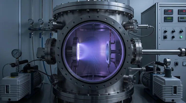
At its core, cathode sputtering is a physical vapor deposition (PVD) technique used to create ultra-thin films. The process uses high-energy ions to bombard a source material, known as the target, physically dislodging atoms from its surface. These ejected atoms then travel through a vacuum and condense onto a separate surface, the substrate, building up a uniform coating atom by atom.
The central principle of cathode sputtering is momentum transfer. By creating a plasma and using an electric field to accelerate ions into a target, the process effectively "sandblasts" the target material on an atomic scale, resulting in a controlled and highly uniform deposition of that material elsewhere.
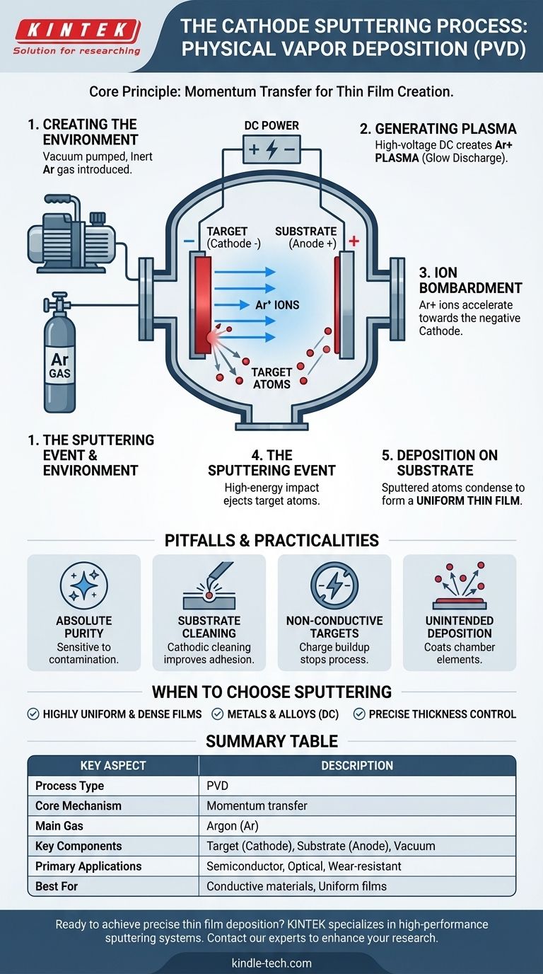
The Core Mechanism: From Plasma to Film
The entire sputtering process takes place within a sealed vacuum chamber. Understanding it involves a clear, five-step sequence that transforms a solid material into a precise thin film.
Step 1: Creating the Environment
Before the process begins, the chamber is pumped down to a very low pressure, creating a vacuum. This is critical to remove air and other contaminants. An inert gas, most commonly Argon (Ar), is then introduced into the chamber at a controlled low pressure.
Step 2: Generating the Plasma
A high-voltage DC electric field is applied between two electrodes: the target material, which acts as the cathode (negative electrode), and the substrate, which acts as the anode (positive electrode). This strong electric field strips electrons from some of the Argon atoms, creating a mix of free electrons and positively charged Argon ions (Ar+). This energized, ionized gas is known as a plasma or "glow discharge."
Step 3: The Ion Bombardment
The positively charged Argon ions (Ar+) are strongly attracted and accelerated towards the negatively charged target (the cathode). They gain significant kinetic energy as they travel across the electric field.
Step 4: The Sputtering Event
Upon impact, the high-energy ions slam into the surface of the target. This collision sets off a "collision cascade," transferring momentum to the atoms within the target material. If the energy transferred to a surface atom is greater than the energy that binds it to the target, that atom is ejected or "sputtered" away.
Step 5: Deposition on the Substrate
The sputtered atoms from the target travel through the low-pressure chamber. They eventually reach the substrate, where they condense on the surface. Over time, this atomic deposition builds up to form a dense, uniform, and high-purity thin film.
Understanding the Pitfalls and Practicalities
While the principle is straightforward, successful sputtering depends on careful control of the process environment and an awareness of its limitations.
The Need for Absolute Purity
The quality of the final film is highly sensitive to contamination. The sputtering gas must be clean and dry to maintain the desired composition of the coating. Likewise, the substrate itself must be pristine to ensure the deposited film adheres properly.
Substrate Cleaning
To improve film adhesion, a technique called cathodic cleaning is often used. Before deposition begins, the voltage polarity is temporarily reversed. This turns the substrate into the cathode, causing it to be bombarded by ions that etch away any surface contaminants.
The Challenge of Non-Conductive Targets
The simple DC sputtering process described here works exceptionally well for conductive materials like metals. However, when sputtering insulating (non-conductive) materials, positive ions accumulate on the target's surface. This charge buildup eventually repels the incoming Argon ions, stopping the sputtering process.
Unintended Deposition
The sputtered material travels in many directions. While most of it coats the substrate, some can end up on other elements within the vacuum chamber. This can alter the chamber's electrical properties over time or even cause short circuits.
When to Choose Cathode Sputtering
Deciding if sputtering is the right method depends on the specific goals of your application.
- If your primary focus is creating highly uniform and dense films: Sputtering excels at depositing thin layers with excellent coverage and strong adhesion across the entire substrate.
- If your primary focus is working with metals and alloys: DC cathode sputtering is a reliable, repeatable, and well-established process for depositing conductive materials.
- If your primary focus is precise control over film thickness: The process offers a very stable and controllable deposition rate, allowing for the creation of films with exact thicknesses down to the atomic level.
Ultimately, cathode sputtering is a foundational technology in modern manufacturing, enabling the production of everything from semiconductor devices to optical coatings and hard-wearing surfaces.
Summary Table:
| Key Aspect | Description |
|---|---|
| Process Type | Physical Vapor Deposition (PVD) |
| Core Mechanism | Momentum transfer via ion bombardment |
| Main Gas Used | Argon (Ar) |
| Key Components | Target (cathode), Substrate (anode), Vacuum chamber |
| Primary Applications | Semiconductor devices, optical coatings, wear-resistant surfaces |
| Best For | Conductive materials, highly uniform and dense films |
Ready to achieve precise thin film deposition in your lab? KINTEK specializes in high-performance sputtering systems and lab equipment designed for researchers and manufacturers who demand superior film quality, uniformity, and process control. Whether you're working with metals, alloys, or advanced materials, our solutions deliver the reliability and precision your laboratory needs. Contact our experts today to discuss how our sputtering technology can enhance your research and production capabilities!
Visual Guide
Related Products
- Chemical Vapor Deposition CVD Equipment System Chamber Slide PECVD Tube Furnace with Liquid Gasifier PECVD Machine
- Reference Electrode Calomel Silver Chloride Mercury Sulfate for Laboratory Use
- Inclined Rotary Plasma Enhanced Chemical Vapor Deposition PECVD Equipment Tube Furnace Machine
- Laboratory CVD Boron Doped Diamond Materials
- Microwave Plasma Chemical Vapor Deposition MPCVD Machine System Reactor for Lab and Diamond Growth
People Also Ask
- What types of substrates are used in CVD to facilitate graphene films? Optimize Graphene Growth with the Right Catalyst
- What are the processes of vapor phase deposition? Understand CVD vs. PVD for Superior Thin Films
- What is the chemical vapor deposition growth process? Build Superior Thin Films from the Atom Up
- What are the advantages of chemical vapor deposition? Achieve Superior Thin Films for Your Lab
- What are the core advantages of PE-CVD in OLED encapsulation? Protect Sensitive Layers with Low-Temp Film Deposition


