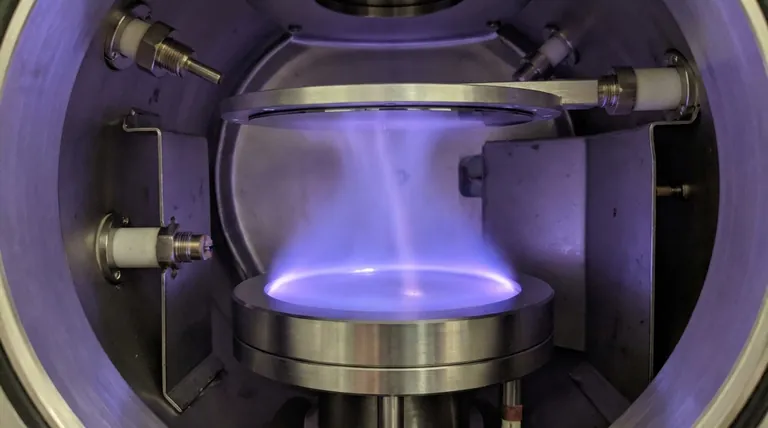
At its core, DC sputtering is a physical vapor deposition (PVD) method that uses energetic ions to dislodge atoms from a source material, known as the target. These dislodged atoms then travel through a vacuum and deposit onto a substrate, forming an exceptionally thin and uniform film. The entire process is driven by a high-voltage direct current (DC) electric field.
DC sputtering is best understood as a microscopic, high-energy billiard game. An inert gas is used to create ion "cue balls," which are accelerated by an electric field to strike a target, knocking loose the target's atoms, which then coat a nearby substrate.
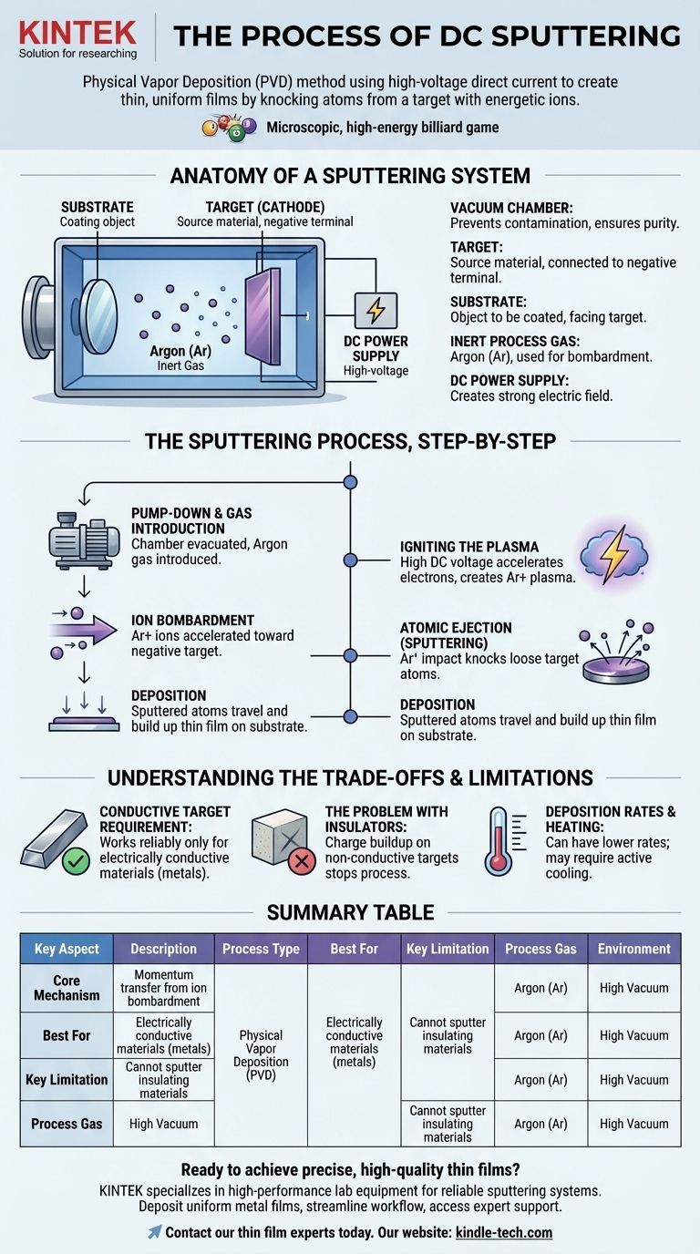
The Anatomy of a Sputtering System
To understand the process, you must first understand the key components of the system, all of which are housed within a vacuum chamber.
The Vacuum Chamber
The process occurs in a high vacuum to prevent sputtered atoms from colliding with air molecules and to eliminate contamination from the final film. A clean environment is critical for film purity and adhesion.
The Target (Cathode)
This is the source material you wish to deposit as a thin film, such as titanium or aluminum. In a DC system, the target is connected to the negative terminal of a power supply, making it the cathode.
The Substrate
This is the object you intend to coat, which could be a silicon wafer, a piece of glass, or a medical implant. It is positioned to face the target to intercept the flow of sputtered material. It is typically at or near the potential of the chamber wall (the anode).
The Inert Process Gas
An inert gas, most commonly Argon (Ar), is bled into the vacuum chamber at a low pressure. This gas is not part of the final film; its purpose is to be ionized and used as the bombardment medium.
The DC Power Supply
A high-voltage DC power supply creates a strong electric field between the target (cathode) and the chamber walls (anode). This field is the engine that drives the entire process.
The Sputtering Process, Step-by-Step
The deposition process follows a precise sequence of events driven by fundamental physics.
Step 1: Pump-Down and Gas Introduction
First, the chamber is evacuated to a high vacuum to remove ambient gases like oxygen and water vapor. Then, a small, precisely controlled amount of Argon gas is introduced.
Step 2: Igniting the Plasma
A high DC voltage is applied between the target and the anode. This powerful electric field accelerates stray free electrons present in the chamber. These high-speed electrons collide with neutral Argon atoms, knocking an electron off and creating a positively charged Argon ion (Ar+) and another free electron. This collision cascade quickly creates a self-sustaining, glowing cloud of ions and electrons known as a plasma.
Step 3: Ion Bombardment
The newly formed, positively charged Argon ions (Ar+) are now strongly accelerated by the electric field directly toward the negatively charged target. They impact the target surface with significant kinetic energy.
Step 4: Atomic Ejection (Sputtering)
The impact of an Argon ion is a pure momentum transfer event. The ion's energy is transferred to the atoms on the target's surface, and if the energy is sufficient to overcome the material's binding energy, one or more target atoms are physically knocked loose or "sputtered."
Step 5: Deposition
These sputtered, neutral target atoms travel in a straight line through the vacuum until they strike a surface. When they land on the substrate, they condense, bond to the surface, and gradually build up, atom by atom, into a dense and uniform thin film.
Understanding the Trade-offs and Limitations
While powerful, DC sputtering is not a universal solution. Understanding its limitations is key to using it effectively.
The Conductive Target Requirement
The most significant limitation of DC sputtering is that it works reliably only for electrically conductive targets, such as metals. Because the target is a cathode, it must be able to dissipate the positive charge delivered by the bombarding ions.
The Problem with Insulators
If you attempt to use a non-conductive (insulating or dielectric) target like a ceramic, positive charge from the Argon ions rapidly accumulates on its surface. This buildup, known as "target poisoning," eventually neutralizes the negative bias, repels incoming ions, and shuts the sputtering process down.
Deposition Rates and Heating
While highly controllable, DC sputtering can have lower deposition rates than other methods like thermal evaporation. The constant ion bombardment also transfers a significant amount of energy into the target and substrate, which may require active cooling for sensitive materials.
Making the Right Choice for Your Goal
Selecting the right deposition method depends entirely on your material and desired outcome.
- If your primary focus is depositing metals or other conductive materials: DC sputtering is an industry-standard, cost-effective, and highly controllable choice for creating high-quality films.
- If your primary focus is film quality, density, and adhesion: The high kinetic energy of sputtered atoms generally produces denser and more adherent films than thermal evaporation.
- If your primary focus is depositing insulating materials (ceramics, oxides): You must use an alternative like Radio Frequency (RF) sputtering, which uses an AC field to avoid the charge buildup that plagues DC sputtering of insulators.
By understanding sputtering as a process of controlled physical momentum transfer, you can effectively engineer surfaces and create materials with precisely tailored properties.
Summary Table:
| Key Aspect | Description |
|---|---|
| Process Type | Physical Vapor Deposition (PVD) |
| Core Mechanism | Momentum transfer from ion bombardment |
| Best For | Electrically conductive materials (metals) |
| Key Limitation | Cannot sputter insulating materials |
| Process Gas | Argon (Ar) |
| Environment | High Vacuum |
Ready to achieve precise, high-quality thin films in your lab?
DC sputtering is a cornerstone technique for depositing conductive coatings, but selecting the right equipment is critical for success. KINTEK specializes in high-performance lab equipment and consumables, providing reliable sputtering systems tailored to your research and production goals.
We help you:
- Deposit uniform metal films with excellent adhesion and density.
- Streamline your workflow with reliable, easy-to-use systems.
- Access expert support to optimize your process and materials.
Let's discuss your specific application. Contact our thin film experts today to find the perfect sputtering solution for your laboratory needs.
Visual Guide
Related Products
- Spark Plasma Sintering Furnace SPS Furnace
- Multi Heating Zones CVD Tube Furnace Machine Chemical Vapor Deposition Chamber System Equipment
- Circulating Water Vacuum Pump for Laboratory and Industrial Use
- Vacuum Induction Melting Spinning System Arc Melting Furnace
People Also Ask
- What is the difference between spark plasma sintering and flash sintering? A Guide to Advanced Sintering Methods
- What are the advantages of CAMI/SPS for W-Cu composite preparation? Reduce cycles from hours to seconds.
- Why are Spark Plasma Sintering (SPS) furnaces or hot presses utilized in the preparation of Li3PS4 solid electrolytes?
- What is the mechanism of SPS process? A Deep Dive into Rapid, Low-Temperature Sintering
- What are the fundamentals of spark plasma sintering process? Unlock Rapid, High-Performance Material Consolidation


