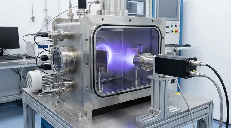
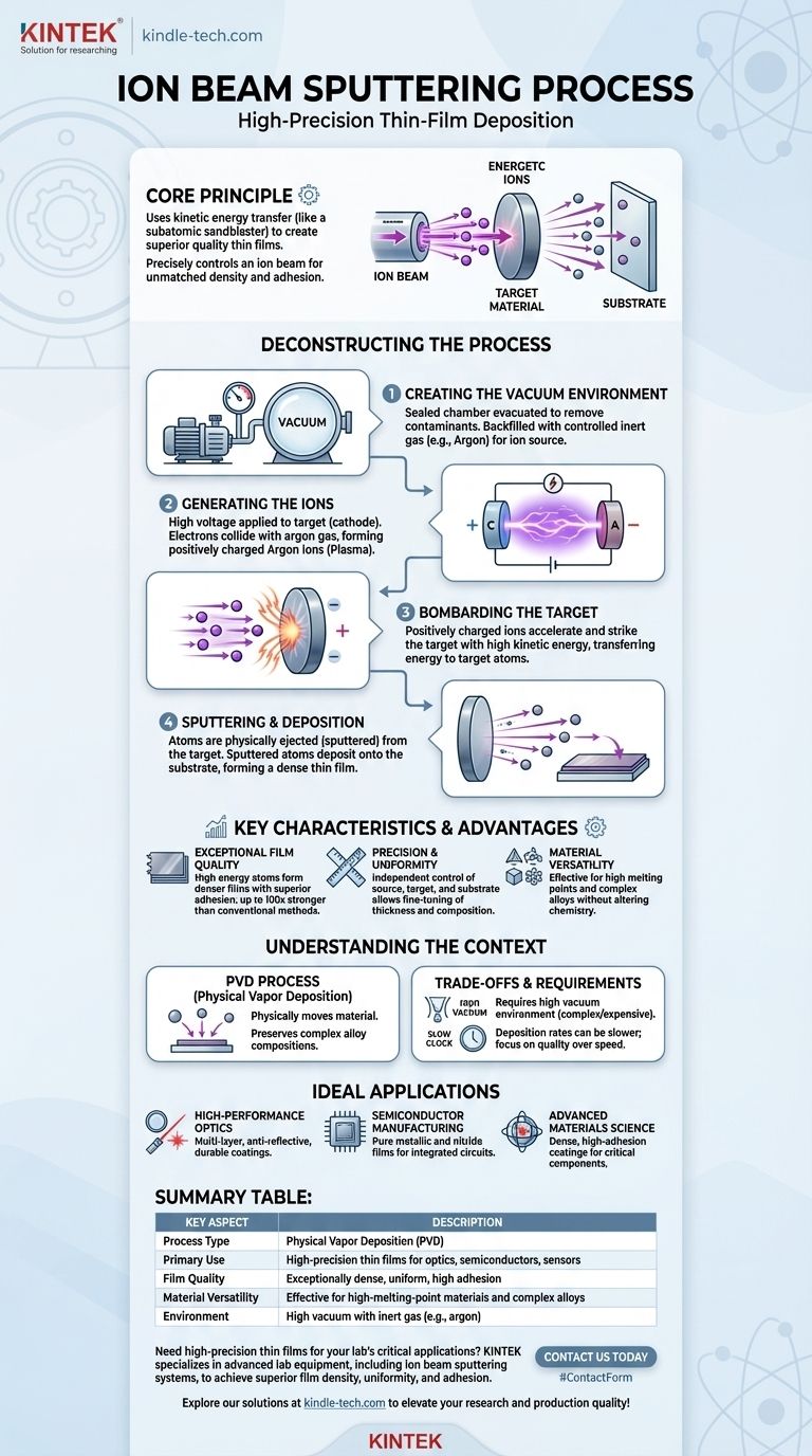
In essence, ion beam sputtering is a high-precision thin-film deposition technique where a focused beam of energetic ions is used to physically dislodge atoms from a source material, known as a target. These dislodged, or "sputtered," atoms then travel through a vacuum and deposit onto a substrate, forming an exceptionally dense and uniform coating.
The core principle of ion beam sputtering is using kinetic energy transfer—like a subatomic sandblaster—to create superior quality thin films. By precisely controlling an ion beam, this method achieves a level of film density and adhesion that other techniques struggle to match.
Deconstructing the Ion Beam Sputtering Process
To understand how sputtering achieves its results, it's best to break it down into a sequence of distinct physical events that occur within a highly controlled environment.
Step 1: Creating the Vacuum Environment
The entire process takes place inside a sealed vacuum chamber. First, the air is evacuated to remove contaminants like oxygen, nitrogen, and water vapor that could interfere with the film's purity.
Once a high vacuum is achieved, the chamber is backfilled with a small, controlled amount of an inert gas, most commonly argon. This gas provides the atoms that will eventually become the ions for the sputtering beam.
Step 2: Generating the Ions
A high voltage is applied to a target, making it a negatively charged electrode (cathode). This causes free electrons to accelerate away from the target.
These high-speed electrons collide with the neutral argon gas atoms. The force of the collision knocks an electron off the argon atom, transforming it into a positively charged argon ion. This process of ionization creates a glowing gas discharge known as a plasma.
Step 3: Bombarding the Target
The positively charged argon ions are strongly attracted to the negatively charged target material. They accelerate towards the target, striking its surface with significant kinetic energy.
This bombardment is the central action of the sputtering process. The energy from the ion collision is transferred directly to the atoms of the target material.
Step 4: Sputtering and Deposition
If the energy transferred by the incoming ion is greater than the target material's binding energy, atoms are physically ejected from the target's surface. These ejected particles are neutral and travel in a straight line from the target.
These sputtered atoms traverse the vacuum chamber and land on the surface of the substrate (often the anode), gradually building up a thin film layer by layer.
Key Characteristics of Ion Beam Sputtering
The unique physics of the process give ion beam sputtering several distinct advantages, making it the preferred method for demanding applications.
Exceptional Film Quality
The sputtered atoms arrive at the substrate with much higher energy than in simple thermal evaporation. This results in energy bonding properties that can be 100 times stronger than conventional vacuum coating.
This high energy ensures the deposited film is extremely dense, with superior adhesion to the substrate.
Precision and Uniformity
Because the ion source, target, and substrate can be independently controlled, the process offers fine-tuned command over film thickness, composition, and uniformity across the entire substrate.
Material Versatility
Sputtering is a physical process, not a chemical one. This makes it exceptionally effective for depositing materials with very high melting points or complex alloys whose composition must be preserved in the final film.
Understanding the Trade-offs
While powerful, it's important to understand the context in which ion beam sputtering operates to appreciate its specific role.
It Is a Physical Vapor Deposition (PVD) Process
Sputtering is fundamentally a PVD technique. It physically moves material from a solid target to a substrate. This contrasts with Chemical Vapor Deposition (CVD), where gases react on a substrate's surface to form the film. The physical nature of sputtering is what allows for the deposition of complex alloys without altering their chemistry.
The Requirement for High Vacuum
The process demands a significantly higher vacuum level than many CVD methods. This requirement for a cleaner, more controlled environment means the equipment is often more complex and expensive to operate and maintain.
Control Over Deposition Rate
The high degree of control that makes sputtering so precise can also mean that deposition rates are sometimes slower than other mass-production coating methods. The focus is on quality and precision, not necessarily speed.
Making the Right Choice for Your Goal
The decision to use ion beam sputtering is driven by the need for performance and precision that cannot be achieved through other means.
- If your primary focus is high-performance optics: This process is the standard for creating multi-layer, anti-reflective, and highly durable coatings for precision lenses, mirrors, and laser components.
- If your primary focus is semiconductor manufacturing: It is used to deposit the extremely pure and uniform metallic and nitride films required for creating integrated circuits on wafers.
- If your primary focus is advanced materials science: The method excels at creating dense, high-adhesion coatings for mission-critical components like precision gyroscopes and specialized sensors.
Ultimately, ion beam sputtering is the premier technique when the quality, density, and precision of a thin film are absolutely non-negotiable.
Summary Table:
| Key Aspect | Description |
|---|---|
| Process Type | Physical Vapor Deposition (PVD) |
| Primary Use | High-precision thin films for optics, semiconductors, sensors |
| Film Quality | Exceptionally dense, uniform, high adhesion |
| Material Versatility | Effective for high-melting-point materials and complex alloys |
| Environment | High vacuum with inert gas (e.g., argon) |
Need high-precision thin films for your lab's critical applications? KINTEK specializes in advanced lab equipment, including ion beam sputtering systems, to help you achieve superior film density, uniformity, and adhesion for optics, semiconductors, and materials science. Contact us today to explore how our solutions can elevate your research and production quality!
Visual Guide
Related Products
- Spark Plasma Sintering Furnace SPS Furnace
- Chemical Vapor Deposition CVD Equipment System Chamber Slide PECVD Tube Furnace with Liquid Gasifier PECVD Machine
- RF PECVD System Radio Frequency Plasma-Enhanced Chemical Vapor Deposition RF PECVD
- E Beam Crucibles Electron Gun Beam Crucible for Evaporation
- Electron Beam Evaporation Coating Gold Plating Tungsten Molybdenum Crucible for Evaporation
People Also Ask
- What is the process fundamentals of spark plasma sintering? Achieve Rapid, High-Density Material Consolidation
- What technical advantages does a Spark Plasma Sintering (SPS) furnace offer for LZP ceramics? Enhance Ionic Conductivity
- What are the advantages of CAMI/SPS for W-Cu composite preparation? Reduce cycles from hours to seconds.
- Why are Spark Plasma Sintering (SPS) furnaces or hot presses utilized in the preparation of Li3PS4 solid electrolytes?
- What is the pressure for spark plasma sintering? A Guide to Optimizing SPS Parameters


