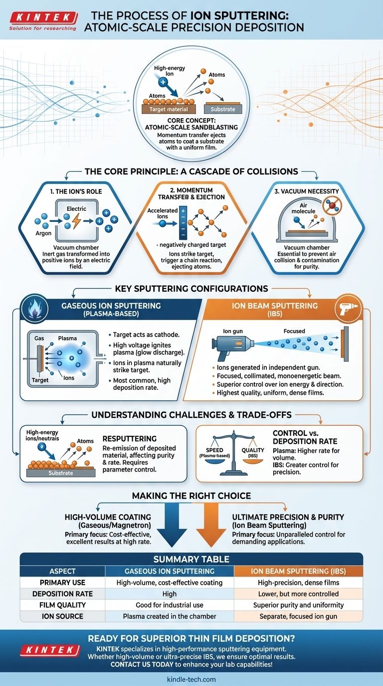
At its core, ion sputtering is a physical deposition process where high-energy ions bombard a target material, physically knocking atoms off its surface. These ejected atoms then travel through a vacuum and deposit onto a substrate, forming an exceptionally thin and uniform film. Think of it as an atomic-scale sandblasting operation.
The central principle of sputtering is momentum transfer. By accelerating ions of an inert gas into a source material (the target), a cascade of atomic collisions ejects individual atoms, which then coat a nearby object (the substrate) with a high-quality thin film.
The Core Principle: A Cascade of Collisions
To understand sputtering, you must first grasp the physics of what happens when a high-energy particle strikes a solid surface. The entire process is orchestrated inside a controlled vacuum environment.
The Role of the Ion
The process begins by introducing an inert gas, typically Argon, into a vacuum chamber. An electric field is applied, which strips electrons from the gas atoms and transforms them into positively charged ions.
These ions become the projectiles in the sputtering process.
Momentum Transfer and Ejection
The positively charged ions are accelerated by an electric field towards the source material, known as the target, which holds a negative charge.
When an ion strikes the target with sufficient energy, it triggers a collision cascade. The ion transfers its momentum to the atoms it hits, which in turn hit other atoms, creating a chain reaction just beneath the target's surface.
If an atom near the surface receives enough energy to overcome its atomic bonding forces, it is physically ejected or "sputtered" from the target.
The Necessity of a Vacuum
This entire process must occur in a vacuum for two critical reasons. First, it prevents the sputtered atoms from colliding with air molecules on their way to the substrate. Second, it prevents contamination and unwanted chemical reactions, ensuring the purity of the deposited film.
Key Sputtering Configurations
While the principle of collision is the same, the method for creating and directing the ions often falls into one of two main configurations.
Gaseous Ion Sputtering (Plasma-Based)
This is the most common configuration. The target itself is used as a cathode (negative electrode) within the low-pressure inert gas.
A high voltage is applied, which ignites the gas into a glow discharge, or plasma. This plasma is a glowing soup of positive ions and free electrons.
The positive ions in the plasma are naturally attracted to the negatively charged target. They accelerate, strike it at high velocity, and initiate the sputtering process.
Ion Beam Sputtering (IBS)
In this more precise method, the ions are generated in a separate ion source or "gun" completely independent of the target material.
This gun creates a highly focused, collimated, and monoenergetic beam of ions, meaning they all have nearly the same energy and direction. This beam is then aimed at the target.
Because the ion energy and direction are so tightly controlled, IBS produces the highest quality, densest, and most uniform films available.
Understanding the Trade-offs and Challenges
Sputtering is a powerful technique, but it is not without its complexities. Understanding its limitations is key to achieving a successful outcome.
The Problem of Resputtering
Resputtering is the re-emission of already-deposited material from the substrate's surface. It can occur when high-energy ions or neutral atoms from the plasma bombard the newly formed film, knocking some of its atoms loose.
This phenomenon can negatively affect the film's purity and deposition rate, requiring careful control over process parameters like pressure and voltage.
Control vs. Deposition Rate
There is often a trade-off between the speed of the process and the quality of the film.
Plasma-based systems typically offer higher deposition rates suitable for industrial production. However, Ion Beam Sputtering provides far greater control over the film's properties, which is critical for sensitive applications like high-performance optics or advanced semiconductors.
Making the Right Choice for Your Goal
Selecting the appropriate sputtering technique depends entirely on the requirements of the final product.
- If your primary focus is cost-effective, high-volume coating: Gaseous or magnetron sputtering is the industry standard, offering excellent results at a high deposition rate.
- If your primary focus is ultimate precision, density, and film purity: Ion Beam Sputtering provides unparalleled control and is the superior choice for demanding applications.
Ultimately, ion sputtering is a versatile and highly controlled method for engineering materials at the atomic level.
Summary Table:
| Aspect | Gaseous Ion Sputtering | Ion Beam Sputtering (IBS) |
|---|---|---|
| Primary Use | High-volume, cost-effective coating | High-precision, dense films |
| Deposition Rate | High | Lower, but more controlled |
| Film Quality | Good for industrial use | Superior purity and uniformity |
| Ion Source | Plasma created in the chamber | Separate, focused ion gun |
Ready to achieve superior thin film deposition in your lab? KINTEK specializes in high-performance sputtering equipment and consumables, offering solutions tailored to your specific research or production needs. Whether you require high-volume coating or ultra-precise Ion Beam Sputtering, our expertise ensures optimal results. Contact us today to discuss how we can enhance your laboratory capabilities!
Visual Guide
Related Products
- Spark Plasma Sintering Furnace SPS Furnace
- Chemical Vapor Deposition CVD Equipment System Chamber Slide PECVD Tube Furnace with Liquid Gasifier PECVD Machine
- RF PECVD System Radio Frequency Plasma-Enhanced Chemical Vapor Deposition RF PECVD
- Customer Made Versatile CVD Tube Furnace Chemical Vapor Deposition Chamber System Equipment
- Vacuum Induction Melting Spinning System Arc Melting Furnace
People Also Ask
- What technical advantages does a Spark Plasma Sintering (SPS) furnace offer for LZP ceramics? Enhance Ionic Conductivity
- Why are Spark Plasma Sintering (SPS) furnaces or hot presses utilized in the preparation of Li3PS4 solid electrolytes?
- What is the mechanism of SPS process? A Deep Dive into Rapid, Low-Temperature Sintering
- What are the advantages of CAMI/SPS for W-Cu composite preparation? Reduce cycles from hours to seconds.
- What is SPS sintering method? A Guide to High-Speed, High-Performance Material Fabrication


