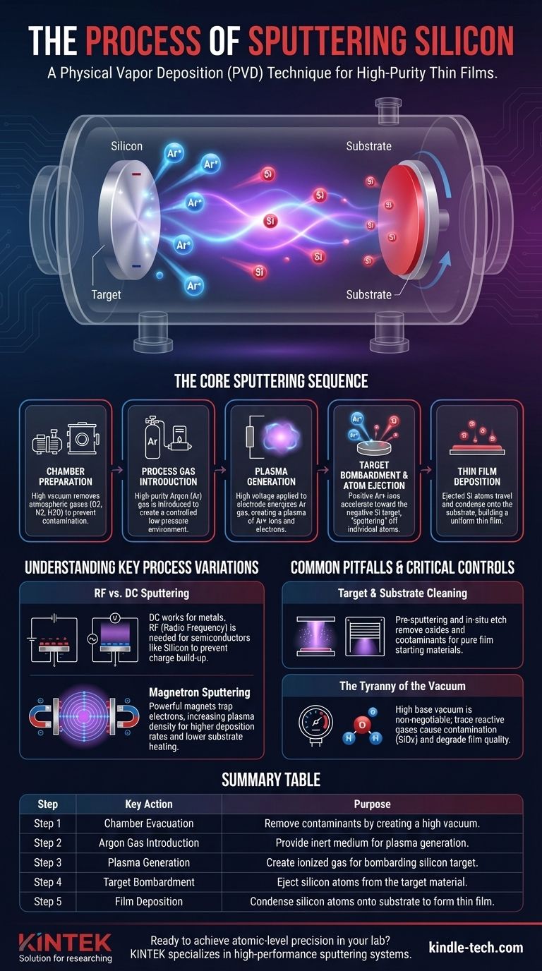
At its core, sputtering silicon is a physical vapor deposition (PVD) technique where a high-purity silicon "target" is bombarded by energetic ions inside a vacuum chamber. This atomic-scale collision ejects silicon atoms from the target, which then travel and condense onto a substrate, forming an exceptionally thin and uniform film.
Sputtering is best understood as a highly controlled process of atomic-scale sandblasting. Instead of sand, it uses ionized gas to chip atoms off a source material and deposit them as a pristine layer on a different surface within a vacuum.
The Core Sputtering Sequence
The sputtering process is a meticulously staged sequence. Each step is designed to control the environment and the energy of the particles to ensure the final silicon film meets precise specifications.
Step 1: Chamber Preparation
The entire process begins by creating an ultra-clean, controlled environment. A substrate (the material to be coated) is placed on a holder and loaded into the sputtering chamber.
The chamber is then sealed and powerful pumps evacuate the air, creating a high vacuum. This crucial step removes atmospheric gases like oxygen, nitrogen, and water vapor, which would otherwise contaminate the silicon film.
Step 2: Process Gas Introduction
Once the required vacuum level is reached, a high-purity inert gas—most commonly Argon (Ar)—is introduced into the chamber.
The system precisely regulates the gas flow to maintain a stable, low-pressure environment, typically in the milliTorr range. This Argon gas will not chemically react with the silicon; it serves only as the medium for bombardment.
Step 3: Plasma Generation
A high voltage is applied to an electrode within the chamber, and the silicon target material is given a negative charge. This strong electric field energizes the Argon gas, stripping electrons from the atoms and creating a plasma.
This plasma is a glowing, ionized gas consisting of positively charged Argon ions (Ar+) and free electrons. It is the engine that drives the entire sputtering process.
Step 4: Target Bombardment and Atom Ejection
The positively charged Argon ions in the plasma are aggressively attracted to the negatively charged silicon target. They accelerate toward the target and strike its surface with significant kinetic energy.
This impact has enough force to physically knock out, or "sputter," individual atoms of silicon from the target, sending them traveling through the vacuum chamber.
Step 5: Thin Film Deposition
The sputtered silicon atoms travel in a straight line from the target until they strike the substrate. Upon hitting the cooler substrate surface, they condense and stick, gradually building up a layer atom by atom.
Over time, this process forms a highly uniform and dense thin film of silicon across the entire substrate surface.
Understanding Key Process Variations
While the core sequence is consistent, several enhancements are critical for effectively sputtering silicon, which is a semiconductor material.
RF vs. DC Sputtering
For conductive metal targets, a simple Direct Current (DC) voltage is effective. However, silicon is a semiconductor. Using DC power can cause a positive charge to build up on the target's surface, eventually repelling the Argon ions and stopping the process.
To overcome this, Radio Frequency (RF) sputtering is used. The rapidly alternating AC voltage effectively cleans the target surface of charge build-up on each cycle, allowing the process to be sustained efficiently for semiconducting and insulating materials.
The Role of Magnetron Sputtering
Modern systems almost always employ magnetron sputtering. This involves placing powerful magnets behind the silicon target.
These magnets create a magnetic field that traps the free electrons from the plasma close to the target surface. The trapped electrons are forced to travel in a spiral path, dramatically increasing their chances of colliding with and ionizing Argon atoms. This results in a much denser plasma, leading to significantly higher sputtering rates and less unwanted heating of the substrate.
Common Pitfalls and Critical Controls
The quality of a sputtered silicon film is entirely dependent on meticulous process control. Overlooking key details can lead to failed depositions.
Target and Substrate Cleaning
The process is only as clean as its starting materials. Before deposition begins, a pre-sputtering step is often performed where the target is sputtered for a short time while a shutter protects the substrate. This removes any oxide layer or contaminants from the target's surface.
Similarly, the substrate itself may undergo an in-situ etch using the plasma to remove any native oxides or organic residue before the shutter is opened for deposition.
The Tyranny of the Vacuum
Even trace amounts of reactive gases like oxygen or water in the chamber can be incorporated into the growing silicon film, creating silicon oxide (SiOx) and ruining its electrical or optical properties. Achieving and maintaining a high base vacuum before introducing the Argon gas is non-negotiable for high-purity films.
Making the Right Choice for Your Goal
The specific parameters of the sputtering process are adjusted based on the desired outcome for the silicon film.
- If your primary focus is film purity: Prioritize achieving the lowest possible base pressure in your chamber and use the highest-grade Argon gas available.
- If your primary focus is deposition speed: Ensure you are using a magnetron sputtering source and optimize the Argon pressure and applied power to maximize the sputtering rate.
- If your primary focus is film uniformity: Control the target-to-substrate distance and incorporate substrate rotation during deposition to average out any inconsistencies.
Ultimately, mastering silicon sputtering is about precisely controlling a volatile plasma environment to achieve atomic-level construction.
Summary Table:
| Step | Key Action | Purpose |
|---|---|---|
| 1 | Chamber Evacuation | Remove contaminants by creating a high vacuum |
| 2 | Argon Gas Introduction | Provide inert medium for plasma generation |
| 3 | Plasma Generation | Create ionized gas for bombarding silicon target |
| 4 | Target Bombardment | Eject silicon atoms from the target material |
| 5 | Film Deposition | Condense silicon atoms onto substrate to form thin film |
| Key Variations | RF Sputtering & Magnetron Enhancement | Enable efficient silicon deposition and higher rates |
Ready to achieve atomic-level precision in your lab? KINTEK specializes in high-performance sputtering systems and lab equipment designed for semiconductor research and thin-film deposition. Our expertise ensures you get the pure, uniform silicon films your projects demand. Contact our experts today to discuss your specific laboratory needs and how we can enhance your research capabilities with reliable, cutting-edge solutions.
Visual Guide
Related Products
- Silicon Carbide (SIC) Ceramic Sheet Wear-Resistant Engineering Advanced Fine Ceramics
- Silicon Carbide (SIC) Ceramic Sheet Flat Corrugated Heat Sink for Engineering Advanced Fine Ceramics
- Precision Machined Silicon Nitride (SiN) Ceramic Sheet for Engineering Advanced Fine Ceramics
- Silicon Carbide (SIC) Ceramic Plate for Engineering Advanced Fine Ceramics
People Also Ask
- What are the uses of silicon carbide ceramics in different industries? Master Extreme Performance in Aerospace, Semiconductors & More
- What is the type of silicon carbide? A Guide to Polymorphs, Grades, and Applications
- What is the strongest ceramics? Silicon Carbide Leads in Hardness & Thermal Strength
- What are the applications of silicon carbide? From Abrasives to High-Tech Semiconductors
- What is the temperature resistance of silicon carbide? Withstands Extreme Heat Up to 1500°C


