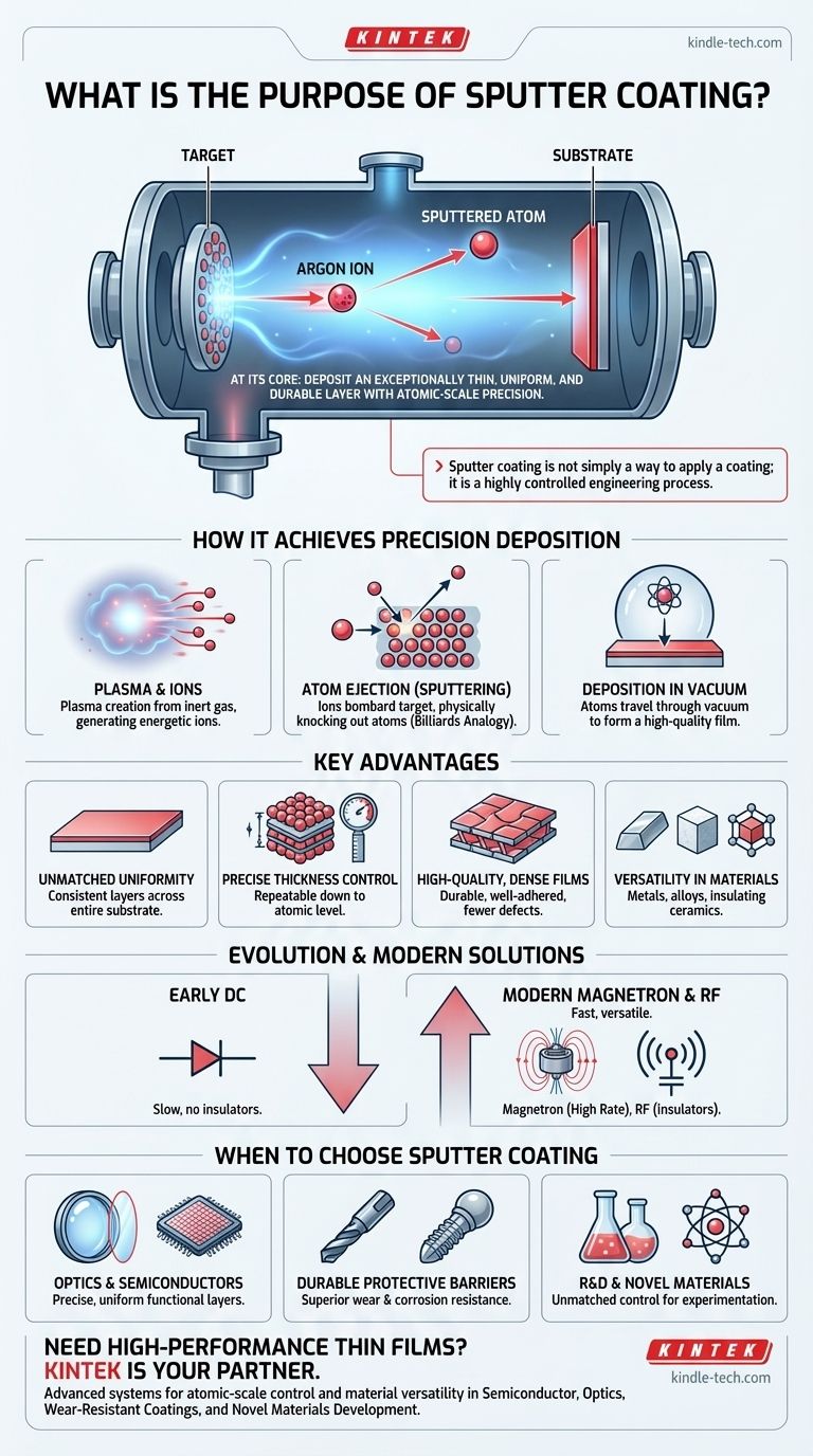
At its core, the purpose of sputter coating is to deposit an exceptionally thin, uniform, and durable layer of material onto a substrate. This physical vapor deposition (PVD) process works by using energetic ions to physically eject atoms from a source material, or "target," which then travel and condense onto the substrate to form a high-quality film.
Sputter coating is not simply a way to apply a coating; it is a highly controlled engineering process. Its true purpose is to achieve a level of atomic-scale precision, uniformity, and material integrity that simpler chemical or thermal deposition methods cannot match.
How Sputter Coating Achieves Precision Deposition
To understand the purpose of sputtering, you must first understand its mechanism. The process relies on a delicate balance of physics within a vacuum chamber to achieve its results.
The Role of Plasma and Ions
First, the chamber is pumped down to a vacuum and backfilled with a small amount of an inert gas, typically argon. An electrical field is then applied, causing the gas to form a plasma—a state of matter containing free electrons and positive ions.
These positively charged argon ions are accelerated by the electric field, directing them with significant force toward the target.
Ejecting Atoms from the Target
The target is a block of the material you wish to deposit. When the high-energy argon ions bombard the target's surface, they physically knock out, or "sputter," individual atoms from the target.
Think of it as a subatomic game of billiards. The argon ion is the cue ball, striking the racked atoms of the target material and sending them scattering. These ejected atoms fly away from the target with high kinetic energy.
Deposition in a Controlled Vacuum
The sputtered atoms travel through the vacuum chamber and land on the substrate (the object being coated), gradually building up a thin film.
The vacuum is critical for two reasons. First, it ensures the sputtered atoms have a clear, unimpeded path to the substrate. Second, the pressure must be perfectly balanced—high enough to sustain the plasma but low enough to prevent sputtered atoms from colliding with gas molecules, which would slow them down and disrupt uniform deposition.
Key Advantages Over Other Methods
The "why" behind sputter coating becomes clear when you examine its distinct advantages, which make it indispensable for high-performance applications.
Unmatched Uniformity and Thickness Control
Because the source is a large-area target and the plasma is stable, the deposition of atoms is incredibly uniform across the entire substrate.
Furthermore, the film's thickness is directly proportional to the deposition time. This allows for precise, repeatable control down to the level of individual atomic layers.
High-Quality, Dense Films
The high kinetic energy of the sputtered atoms helps create films that are exceptionally dense and well-adhered to the substrate. This results in coatings that are far more durable and have fewer defects than those applied by other methods.
This process also allows for creating dense films with reduced internal stress, even at low deposition temperatures (below 150 °C).
Versatility in Materials
Unlike some processes that are limited to metals, sputtering can deposit a vast range of materials. This includes metals, alloys, and even insulating ceramic compounds. This versatility makes it a cornerstone of modern materials science and manufacturing.
Understanding the Trade-offs and Evolution
No technology is without its challenges, and understanding them reveals why modern sputtering systems have evolved.
The Challenge of Deposition Rate
Early, simple DC diode sputtering systems were effective but suffered from a low deposition rate. This made the process slow and less economical for mass production.
Historical Inability to Sputter Insulators
Those same early DC systems could not sputter insulating materials. A charge would build up on the surface of an insulating target, effectively repelling the positive ions and stopping the sputtering process.
Modern Solutions: Magnetron and RF Sputtering
Modern techniques overcome these issues. Magnetron sputtering uses powerful magnets to trap electrons near the target, dramatically increasing the efficiency of ion creation and leading to much higher deposition rates.
RF (Radio Frequency) sputtering uses an alternating current to prevent charge buildup on insulating targets, enabling the deposition of ceramics and other non-conductive materials.
When to Choose Sputter Coating
You should turn to sputter coating when the performance and quality of the thin film are the primary concerns.
- If your primary focus is high-performance optics or semiconductors: Sputter coating is essential for creating the precise, uniform anti-reflective, conductive, or dielectric layers these components require.
- If your primary focus is creating a durable, protective barrier: The dense, well-adhered films from sputtering provide superior wear and corrosion resistance on everything from cutting tools to medical implants.
- If your primary focus is research and development: Sputtering offers unmatched control over film thickness and composition, making it a critical tool for experimenting with and fabricating novel materials.
Ultimately, you choose sputter coating when the quality, uniformity, and performance of the deposited film are non-negotiable.
Summary Table:
| Key Feature | Benefit |
|---|---|
| Unmatched Uniformity | Creates consistent, even layers across the entire substrate surface. |
| Precise Thickness Control | Allows for repeatable deposition down to the atomic layer. |
| Dense, High-Quality Films | Results in durable, well-adhered coatings with fewer defects. |
| Versatile Material Deposition | Capable of coating with metals, alloys, and insulating ceramics. |
Need High-Performance Thin Films for Your Lab?
When the quality and precision of your coatings are non-negotiable, KINTEK is your partner. Our advanced sputter coating systems are engineered to deliver the atomic-scale control, uniformity, and material versatility that your R&D or production demands.
We specialize in providing lab equipment and consumables for:
- Semiconductor and Microelectronics Fabrication
- Advanced Optics and Photonics Research
- Wear-Resistant and Protective Coatings
- Novel Materials Development
Let us help you achieve superior results. Contact our experts today to discuss your specific application and find the perfect sputtering solution for your laboratory's needs.
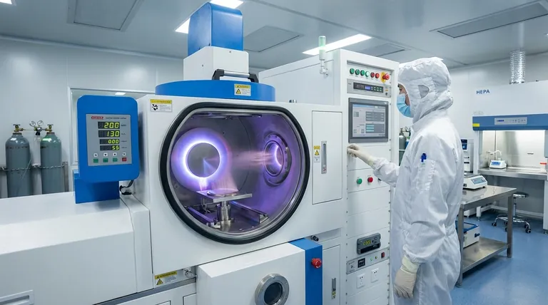
Visual Guide
Related Products
- Infrared Transmission Coating Sapphire Sheet Substrate Window
- Electron Beam Evaporation Coating Oxygen-Free Copper Crucible and Evaporation Boat
- 400-700nm Wavelength Anti Reflective AR Coating Glass
- Custom CVD Diamond Coating for Lab Applications
- Molybdenum Tungsten Tantalum Special Shape Evaporation Boat
People Also Ask
- How can we create a reducing environment? Master the Methods for Precise Chemical Control
- What is organic thin film? A Guide to Engineered Molecular Layers for Advanced Tech
- What is optical coating used for? Control Light for Enhanced Performance in Your Applications
- Is Sputter Tint good? Premium Heat Rejection & Long-Term Durability Explained
- Why do we need optical coating? To Control Light and Enhance Optical Performance


