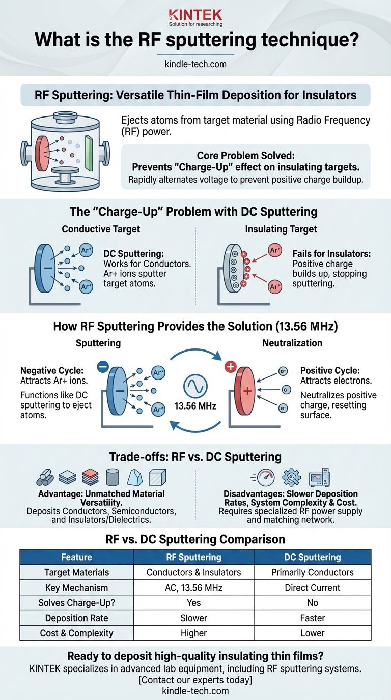
In short, RF sputtering is a versatile thin-film deposition technique that uses a radio frequency (RF) power source to eject atoms from a target material onto a substrate. Unlike simpler DC sputtering, this method is uniquely capable of depositing thin films from materials that do not conduct electricity, such as ceramics and oxides.
The core problem RF sputtering solves is the "charge-up" effect that occurs when trying to sputter insulating materials. By rapidly alternating the voltage, it prevents a positive charge from building up on the target, allowing for the continuous, stable deposition of non-conductive thin films.
The Fundamental Challenge: Sputtering Insulators
How Basic Sputtering Works
Sputtering is a type of Physical Vapor Deposition (PVD). The process takes place in a vacuum chamber filled with an inert gas, typically argon.
A high voltage is applied to create a plasma, which is an energized state of the argon gas containing positive argon ions (Ar+) and free electrons.
These energetic positive ions are accelerated toward a source material, known as the target. They bombard the target with enough force to knock atoms loose, a process called "sputtering." These ejected target atoms then travel through the chamber and deposit onto a substrate (like a silicon wafer or piece of glass), building up a thin film.
The "Charge-Up" Problem with DC Sputtering
In the simplest form, Direct Current (DC) sputtering, the target is given a constant negative voltage to attract the positive argon ions. This works perfectly for conductive targets, like metals.
However, if the target is an insulating material (a dielectric), this process quickly fails. The constant bombardment by positive ions causes a positive charge to accumulate on the target's surface. Since the material cannot conduct this charge away, the surface eventually becomes so positive that it repels the incoming argon ions, stopping the sputtering process entirely.
How RF Sputtering Provides the Solution
The Role of an Alternating Current (AC)
RF sputtering solves the charge-up problem by replacing the constant DC voltage with a high-frequency Alternating Current (AC) power source. This rapidly flips the voltage on the target from negative to positive.
The industry-standard frequency used is 13.56 MHz, which is fast enough to prevent charge buildup while efficiently sustaining the plasma.
The Negative Cycle: Sputtering the Material
During the negative half of the AC cycle, the target is negatively charged. This functions just like DC sputtering.
The negative potential attracts the heavy, positive argon ions from the plasma, which bombard the target and sputter atoms away for deposition onto the substrate.
The Positive Cycle: Neutralizing the Surface
During the brief positive half of the cycle, the target becomes positively charged.
Instead of attracting sputtering ions, this positive potential now attracts lightweight, highly mobile electrons from the plasma. These electrons flood the target surface, instantly neutralizing any positive charge that accumulated during the previous negative cycle. This "resets" the surface, making it ready for the next sputtering cycle.
Understanding the Trade-offs
Advantage: Unmatched Material Versatility
The primary advantage of RF sputtering is its ability to deposit virtually any material, including metals, semiconductors, and most importantly, insulators and dielectrics. This makes it essential for applications like optical coatings and semiconductor manufacturing.
Disadvantage: Slower Deposition Rates
Generally, RF sputtering has a lower deposition rate compared to DC sputtering. The positive cycle is for neutralization, not deposition, which reduces overall efficiency. For depositing simple conductive metals, DC sputtering is often a much faster and more cost-effective choice.
Disadvantage: System Complexity and Cost
An RF sputtering system is more complex than a DC system. It requires a specialized RF power supply and an impedance matching network to efficiently transfer power to the plasma. This added complexity increases the overall cost of the equipment.
Making the Right Choice for Your Goal
- If your primary focus is depositing a conductive material (e.g., gold, aluminum, titanium): DC sputtering is typically the faster, simpler, and more economical method.
- If your primary focus is depositing an insulating material (e.g., silicon dioxide, aluminum oxide, titanium nitride): RF sputtering is the necessary and standard technique to avoid the charge-up effect.
- If your primary focus is creating films from complex alloys or high-melting-point materials: Sputtering in general (both RF and DC) is a superior method compared to thermal evaporation, offering better film adhesion and composition control.
Ultimately, RF sputtering is an indispensable tool that enables the creation of advanced materials and devices by overcoming the fundamental electrical limitations of insulators.
Summary Table:
| Feature | RF Sputtering | DC Sputtering |
|---|---|---|
| Target Materials | Conductors & Insulators (e.g., ceramics, oxides) | Primarily Conductors (e.g., metals) |
| Key Mechanism | Alternating Current (AC, 13.56 MHz) | Direct Current (DC) |
| Solves Charge-Up? | Yes | No |
| Deposition Rate | Slower | Faster |
| Cost & Complexity | Higher | Lower |
Ready to deposit high-quality insulating thin films? KINTEK specializes in advanced lab equipment, including RF sputtering systems. Our solutions provide the precise control and reliability your laboratory needs for research and development. Contact our experts today to discuss how we can support your specific project requirements.
Visual Guide
Related Products
- RF PECVD System Radio Frequency Plasma-Enhanced Chemical Vapor Deposition RF PECVD
- Spark Plasma Sintering Furnace SPS Furnace
- Horizontal High Temperature Graphite Vacuum Graphitization Furnace
People Also Ask
- What is plasma chemical vapor deposition? A Low-Temperature Thin Film Coating Solution
- How does Radio Frequency Enhanced Plasma Chemical Vapour Deposition (RF-PECVD) work? Learn the Core Principles
- What is plasma enhanced chemical vapour deposition process? Unlock Low-Temperature, High-Quality Thin Films
- What is plasma enhanced chemical vapour deposition PECVD used for? Enable Low-Temp Thin Films for Electronics & Solar
- What is the role of RF-PECVD in VFG preparation? Mastering Vertical Growth and Surface Functionality


