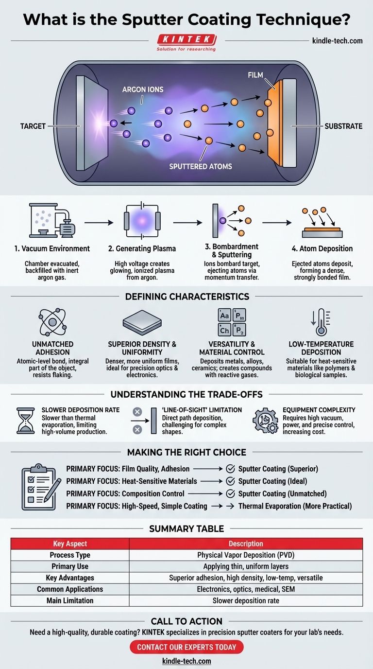
At its core, sputter coating is a physical vapor deposition (PVD) technique used to apply an exceptionally thin and uniform layer of material onto a surface. It works by creating a plasma in a vacuum and using ions from that plasma to bombard a source material, known as a "target." This collision ejects atoms from the target, which then travel and deposit onto the object being coated, forming a durable, high-quality film atom-by-atom.
Sputter coating is not simply a method of applying a layer; it is an atomic-level bombardment process. This momentum transfer integrates the coating material into the substrate's surface, resulting in films with superior adhesion, density, and uniformity compared to many other coating techniques.
How Sputtering Works: From Plasma to Film
Understanding the sputter coating process involves four distinct stages that occur within a controlled vacuum chamber.
The Vacuum Environment
First, the object to be coated (the substrate) and the material to be deposited (the target) are placed in a vacuum chamber. All air is pumped out, creating a near-vacuum.
The chamber is then backfilled with a small, controlled amount of an inert gas, most commonly argon.
Generating the Plasma
A high voltage is applied between the target and the chamber walls. This electrical energy strips electrons from the argon atoms, creating a plasma—a glowing, ionized gas consisting of positive argon ions and free electrons.
The Bombardment Process
The target is given a negative charge, causing the positively charged argon ions in the plasma to accelerate and bombard its surface with significant force.
This energetic collision is a momentum transfer process. The impact of the argon ions physically knocks out, or "sputters," individual atoms from the target material.
Deposition onto the Substrate
The sputtered atoms travel through the vacuum chamber and land on the substrate. Because these atoms are ejected with high energy, they embed themselves into the substrate's surface, forming an incredibly strong bond.
Over time, these deposited atoms build up to form a thin, dense, and highly uniform film across the substrate.
The Defining Characteristics of a Sputtered Film
Sputtering is chosen for its unique advantages, which result in films with properties that are difficult to achieve with other methods.
Unmatched Adhesion
Because the sputtered particles are driven into the substrate with high energy, the bond is formed at an atomic level. The coating becomes an integral part of the object rather than just a superficial layer, offering exceptional durability and resistance to flaking.
Superior Density and Uniformity
The process creates films that are much denser and more uniform than those from other methods like vacuum evaporation. This allows for the creation of extremely thin, continuous films—sometimes less than 10 nanometers thick—making it ideal for precision applications in electronics and optics.
Versatility and Material Control
Sputtering can deposit a vast range of materials, including pure metals, alloys, and even insulating ceramics. By introducing reactive gases like oxygen or nitrogen into the chamber, you can also create compound films, such as oxides and nitrides.
Low-Temperature Deposition
The process itself does not significantly heat the substrate. This makes sputter coating one of the best methods for coating heat-sensitive materials like plastics, polymers, and delicate biological samples for analysis in a scanning electron microscope (SEM).
Understanding the Trade-offs
No technique is perfect. To use sputter coating effectively, you must be aware of its inherent limitations.
Deposition Rate vs. Other Methods
Sputtering is generally a slower process compared to thermal evaporation. The atom-by-atom bombardment is highly controlled but takes longer to build up a thick film, which can be a limiting factor in high-volume production.
The 'Line-of-Sight' Limitation
In its basic form, sputtering is a line-of-sight process. The sputtered atoms travel in a relatively straight line from the target to the substrate. Coating highly complex shapes with deep undercuts or internal surfaces can be challenging without sophisticated substrate rotation and manipulation.
Equipment and Process Complexity
Sputter coating systems require a significant investment. The need for a high-vacuum environment, high-voltage power supplies, and precise gas control makes the equipment and operation more complex and costly than simpler coating methods.
Making the Right Choice for Your Goal
Selecting a coating technology depends entirely on your specific requirements for film quality, material compatibility, and production efficiency.
- If your primary focus is film quality and adhesion: Sputter coating is superior for creating dense, durable, and strongly bonded films for critical applications in electronics, optics, or medical devices.
- If your primary focus is coating heat-sensitive materials: The low-temperature nature of sputtering makes it the ideal choice for polymers, plastics, or biological specimens that would be damaged by other methods.
- If your primary focus is composition control: Sputtering offers unmatched precision in depositing complex alloys or creating compound films by mixing gases, which is vital for advanced materials research.
- If your primary focus is high-speed, simple coating: For less demanding applications where ultimate film quality is not critical, the higher speed and lower cost of thermal evaporation may be a more practical choice.
Ultimately, choosing sputter coating is a decision to prioritize precision, quality, and adhesion over sheer deposition speed.
Summary Table:
| Key Aspect | Description |
|---|---|
| Process Type | Physical Vapor Deposition (PVD) |
| Primary Use | Applying thin, uniform layers of material onto a substrate |
| Key Advantages | Superior adhesion, high film density, low-temperature deposition, versatility with materials |
| Common Applications | Electronics, optics, medical devices, SEM sample preparation |
| Main Limitation | Slower deposition rate compared to methods like thermal evaporation |
Need a high-quality, durable coating for your lab's materials?
KINTEK specializes in providing precision lab equipment, including sputter coaters, to help you achieve superior thin films with excellent adhesion and uniformity. Whether you're working with sensitive polymers, advanced alloys, or require precise composition control for your research, our solutions are designed to meet your specific laboratory needs.
Contact our experts today to discuss how our sputter coating technology can enhance your results!
Visual Guide
Related Products
- HFCVD Machine System Equipment for Drawing Die Nano-Diamond Coating
- Electron Beam Evaporation Coating Oxygen-Free Copper Crucible and Evaporation Boat
- 400-700nm Wavelength Anti Reflective AR Coating Glass
People Also Ask
- What are the advantages of chemical vapor deposition? Achieve Superior Thin Films for Your Lab
- What is the function of tungsten filaments in HFCVD? Powering Diamond Film Synthesis with Thermal Excitation
- Why is Chemical Vapor Deposition (CVD) equipment uniquely suited for constructing hierarchical superhydrophobic structures?
- How expensive is chemical vapor deposition? Understanding the True Cost of High-Performance Coating
- What is the chemical vapor deposition growth process? Build Superior Thin Films from the Atom Up


