At its core, Atomic Layer Deposition (ALD) achieves perfect conformality because it is a surface-controlled process, not a line-of-sight or gas-phase deposition. The film is built one atomic layer at a time through a sequence of self-limiting chemical reactions that occur uniformly on every exposed surface, regardless of its shape or orientation. This ensures that even the deepest trenches and most complex 3D nanostructures are coated with a film of perfectly uniform thickness.
Unlike other methods that "spray" or "rain" material onto a surface, ALD "grows" a film directly from the substrate itself. This is achieved by separating a chemical reaction into two distinct, self-limiting half-reactions, ensuring that exactly one atomic layer is added per cycle, everywhere.
The ALD Cycle: A Tale of Two Half-Reactions
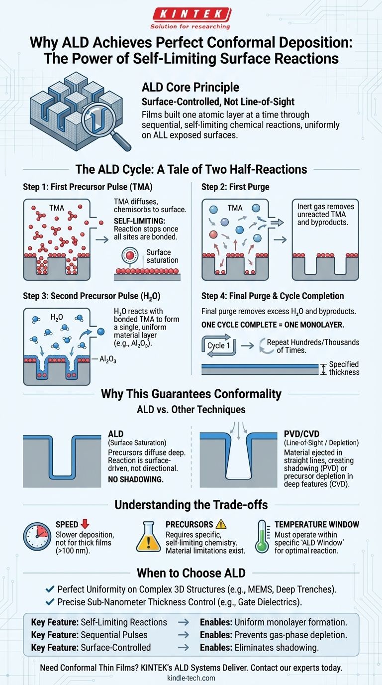
To understand ALD's conformality, you must first understand its fundamental cyclic nature. The process does not deposit material continuously. Instead, it builds a film through a repeated sequence of four distinct steps. Let's use the common example of creating aluminum oxide (Al₂O₃) from Trimethylaluminum (TMA) and water (H₂O).
Step 1: The First Precursor Pulse (TMA)
The process begins by introducing the first chemical, a precursor gas (TMA), into the reaction chamber.
The TMA molecules diffuse throughout the chamber, covering every surface, including the tops, bottoms, and sidewalls of any features on the substrate. They chemically bond (chemisorb) to reactive sites on the surface.
The "Self-Limiting" Principle
This step is self-limiting. Once every available reactive site on the surface has bonded with a TMA molecule, the reaction automatically stops. No more TMA can attach to the surface, and excess molecules remain as a gas. This is the absolute key to ALD's power.
Step 2: The First Purge
Next, an inert gas like nitrogen or argon is flushed through the chamber. This purge completely removes all the excess, unreacted TMA molecules and any gaseous byproducts from the reaction.
Only the single layer of TMA molecules that chemically bonded to the surface remains. This purge step is critical to prevent unwanted gas-phase reactions (i.e., Chemical Vapor Deposition) in the next step.
Step 3: The Second Precursor Pulse (H₂O)
The second precursor, in this case, water vapor (H₂O), is pulsed into the chamber.
These water molecules react only with the layer of TMA molecules already attached to the surface. This reaction forms a single, uniform layer of the desired material, aluminum oxide (Al₂O₃), and prepares the surface with new reactive sites for the next cycle.
Step 4: The Final Purge & Cycle Completion
A final purge with inert gas removes all excess water vapor and the gaseous byproducts from this second reaction.
At the end of these four steps, a single, atomically thin layer of Al₂O₃ has been deposited uniformly across all surfaces. This entire cycle is then repeated hundreds or thousands of times to build the film to the desired thickness.
Why This Mechanism Guarantees Conformality
The sequential and self-limiting nature of the ALD cycle is what fundamentally separates it from other deposition techniques and ensures its superior conformality.
Surface Saturation vs. Line-of-Sight
Techniques like Physical Vapor Deposition (PVD), such as sputtering or evaporation, are line-of-sight. Material is ejected from a source and travels in a straight line to the substrate. This creates a "shadowing" effect, where the tops of features get a thick coating while the sidewalls get very little and the bottoms of trenches may get none at all.
ALD avoids this entirely. The precursor gases can diffuse deep into high-aspect-ratio structures. As long as a gas molecule can reach a surface, it will react and contribute to the film, a process driven by surface chemistry, not directionality.
Uniform Reaction vs. Depletion Effects
Conventional Chemical Vapor Deposition (CVD) can also suffer from non-conformality. In CVD, precursors react together in the gas phase or on the surface continuously. In a deep trench, the reaction can occur faster at the opening than at the bottom, depleting the precursor concentration as it travels deeper.
This results in a film that is thickest at the top and thinnest at the bottom, and can even lead to the opening "pinching off." ALD's self-limiting nature prevents this, as the reaction halts after one monolayer forms, allowing the precursor gas time to fully saturate the entire surface area before the next step begins.
Digital Control Over Thickness
A direct result of this mechanism is that film thickness is determined simply by the number of cycles performed. Each cycle adds a predictable amount of material (e.g., ~1 Ångström of Al₂O₃). This gives engineers precise, digital control over film thickness at the sub-nanometer level.
Understanding the Trade-offs
While its conformality is unmatched, ALD is not the solution for every problem. Understanding its limitations is crucial for making an informed decision.
Deposition Speed
The primary trade-off is speed. Because the film is built one atomic layer at a time, ALD is an inherently slow process compared to PVD or CVD. Depositing a thick film (e.g., >100 nm) can be impractically time-consuming.
Precursor Chemistry and Material Limitations
ALD requires a pair of precursors that exhibit the correct self-limiting reaction chemistry within a shared temperature range. Finding suitable precursors for certain elements or compounds can be a significant research challenge, meaning not all materials can be easily deposited with ALD.
The ALD Temperature Window
The process must operate within a specific temperature range known as the "ALD window." If the temperature is too low, precursors may simply condense on the surface instead of reacting. If it is too high, the precursors may decompose on their own, leading to uncontrolled, CVD-like growth and destroying the self-limiting behavior.
When to Choose ALD
Your choice of deposition method must be guided by the specific requirements of your application.
- If your primary focus is perfect uniformity on complex 3D structures: ALD is the unparalleled choice, essential for applications like coating deep trenches, porous materials, or MEMS devices.
- If your primary focus is precise, sub-nanometer thickness control: ALD's layer-by-layer growth makes it the ideal method for creating the ultra-thin, high-quality gate dielectrics and barrier layers required in modern microelectronics.
- If your primary focus is speed and depositing thick films (>100 nm): You should strongly consider alternatives like CVD or PVD, as ALD's slow deposition rate will likely be a significant bottleneck for your process.
Ultimately, understanding ALD's self-limiting nature empowers you to leverage its unique strengths for the most demanding thin-film applications.
Summary Table:
| Key Feature | How It Enables Conformality |
|---|---|
| Self-Limiting Reactions | Ensures uniform monolayer formation; reaction stops automatically when surface sites are saturated. |
| Sequential Precursor Pulses | Separates chemical reactions into distinct steps, preventing gas-phase depletion and ensuring even coverage. |
| Surface-Controlled Growth | Film grows from the substrate itself, not via line-of-sight deposition, eliminating shadowing effects. |
| Gas Diffusion & Purge Cycles | Precursors diffuse into deep trenches; purges remove excess gas, preventing unwanted reactions. |
Need Conformal Thin Films for Your Advanced Applications?
Whether you're working on next-generation microelectronics, MEMS devices, or coating complex 3D nanostructures, KINTEK's precision ALD systems deliver the perfect uniformity and atomic-level control you require. Our lab equipment and consumables are designed to meet the most demanding thin-film challenges.
Contact our experts today to discuss how our ALD solutions can enhance your research and production processes. Let KINTEK be your partner in achieving superior material performance.
Visual Guide
Related Products
- Chemical Vapor Deposition CVD Equipment System Chamber Slide PECVD Tube Furnace with Liquid Gasifier PECVD Machine
- RF PECVD System Radio Frequency Plasma-Enhanced Chemical Vapor Deposition RF PECVD
- Electron Beam Evaporation Coating Oxygen-Free Copper Crucible and Evaporation Boat
- Hemispherical Bottom Tungsten Molybdenum Evaporation Boat
- Custom CVD Diamond Coating for Lab Applications
People Also Ask
- What happens during deposition chemistry? Building Thin Films from Gaseous Precursors
- What is the chemical vapor deposition growth process? Build Superior Thin Films from the Atom Up
- What are the processes of vapor phase deposition? Understand CVD vs. PVD for Superior Thin Films
- What are the core advantages of PE-CVD in OLED encapsulation? Protect Sensitive Layers with Low-Temp Film Deposition
- What is plasma enhanced chemical vapor deposition PECVD equipment? A Guide to Low-Temperature Thin Film Deposition
