In short, sputtering is required to deposit exceptionally thin, uniform, and high-quality films of a material onto a surface. This physical vapor deposition (PVD) technique is indispensable in industries like semiconductor manufacturing and precision optics because it offers precise control over the coating's thickness, purity, and adhesion.
The core problem that sputtering solves is the need to precisely control the properties of a surface at a near-atomic level. Sputtering is required when other coating methods cannot deliver the necessary uniformity, material versatility, or adhesion for high-performance applications.
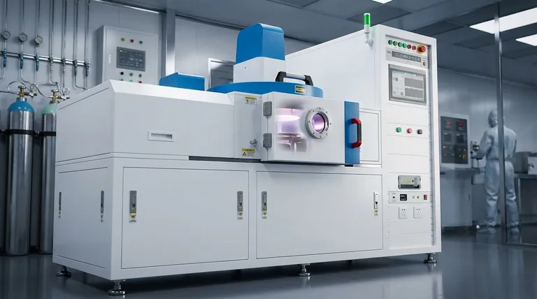
What is Sputtering? A Look at the Core Mechanism
Sputtering is a physical process, not a chemical one. It functions by using momentum to physically knock atoms off a source material and deposit them onto a target surface, building a film one atom at a time within a highly controlled environment.
Creating a Controlled Vacuum
The entire process must occur within a vacuum chamber. This vacuum is critical because it removes air and other particles that could contaminate the film or interfere with the process. This clean environment ensures the sputtered atoms can travel directly to their destination.
Generating a Plasma
An inert gas, most commonly Argon, is introduced into the chamber. A high voltage is then applied, which energizes the gas and strips electrons from the Argon atoms, creating a glowing gaseous plasma—a mixture of positively charged ions (Ar+) and free electrons.
The Bombardment Process
The source material, known as the target, is given a negative electrical charge. This causes the positively charged Argon ions from the plasma to accelerate aggressively towards it. These ions collide with the target with significant force.
Deposition onto the Substrate
This high-energy collision is the sputtering event. The momentum transfer is so great that it physically ejects, or "sputters," individual atoms from the target material. These ejected atoms travel in a straight line through the vacuum and strike the component to be coated, known as the substrate, gradually building a thin, dense film.
The Key Advantages: Why Sputtering is Indispensable
Sputtering isn't just one way to create a coating; for many advanced applications, it is the only way to achieve the required performance due to its unique combination of benefits.
Unmatched Versatility
Sputtering can be used to deposit an incredibly wide range of materials. This includes metals, ceramics, and even plastics. Critically, it works for both electrically conductive and insulating materials, a major advantage over other deposition techniques.
Superior Film Quality
The films produced by sputtering are known for their exceptional quality. They exhibit excellent uniformity across the substrate, are highly dense with fewer defects, and demonstrate strong adhesion because the sputtered atoms embed themselves into the substrate's surface.
High Purity and Precision
Because the process occurs in a high vacuum, the risk of contamination is minimized, resulting in very pure coatings. The rate of deposition can be carefully controlled, allowing for the creation of films with precise thickness, often on the scale of nanometers.
Common Pitfalls and Trade-offs
While powerful, sputtering is a sophisticated process with inherent complexities that make it unsuitable for every coating task.
Slower Deposition Rates
The atom-by-atom nature of sputtering, while precise, is generally slower than bulk coating methods like electroplating or thermal spraying. This can make it less efficient for applications requiring very thick films.
Complex and Expensive Equipment
Sputtering systems require a significant investment. The need for high-vacuum chambers, specialized power supplies, and sophisticated process controls makes the equipment complex to operate and maintain.
Line-of-Sight Limitation
Because sputtered atoms travel in a straight line from the target to the substrate, it can be challenging to uniformly coat complex, three-dimensional shapes with deep recesses or hidden surfaces.
Making the Right Choice for Your Goal
Selecting sputtering is a decision driven by the end-use requirements of the coated component.
- If your primary focus is material versatility: Sputtering is the definitive choice for depositing high-performance insulating materials or complex alloys that other methods can't handle.
- If your primary focus is high-performance coatings: The process is required for applications in semiconductors, optics, and medical devices where film uniformity, density, and adhesion are critical to function.
- If your primary focus is achieving high purity: The vacuum-based nature of sputtering makes it the ideal process for creating films where any level of contamination would cause failure.
Ultimately, sputtering is the required choice when the performance, purity, and precision of a surface are non-negotiable.
Summary Table:
| Aspect | Why Sputtering is Required |
|---|---|
| Film Quality | Creates exceptionally uniform, dense, and high-adhesion coatings. |
| Material Versatility | Deposits both conductive and insulating materials (metals, ceramics, plastics). |
| Precision & Purity | Enables nanometer-level thickness control in a contamination-free vacuum. |
| Key Applications | Semiconductor manufacturing, precision optics, medical devices. |
Need high-precision thin films for your lab? KINTEK specializes in advanced sputtering equipment and consumables for laboratory needs. Our solutions deliver the material versatility, purity, and uniformity your research demands. Contact us today to explore how our expertise can enhance your coating processes!
Visual Guide

Related Products
- Spark Plasma Sintering Furnace SPS Furnace
- Vacuum Induction Melting Spinning System Arc Melting Furnace
- Chemical Vapor Deposition CVD Equipment System Chamber Slide PECVD Tube Furnace with Liquid Gasifier PECVD Machine
- Customer Made Versatile CVD Tube Furnace Chemical Vapor Deposition Chamber System Equipment
People Also Ask
- What is the mechanism of SPS process? A Deep Dive into Rapid, Low-Temperature Sintering
- What is SPS sintering method? A Guide to High-Speed, High-Performance Material Fabrication
- What is the pressure for spark plasma sintering? A Guide to Optimizing SPS Parameters
- What is the difference between spark plasma sintering and flash sintering? A Guide to Advanced Sintering Methods
- What is the process fundamentals of spark plasma sintering? Achieve Rapid, High-Density Material Consolidation


