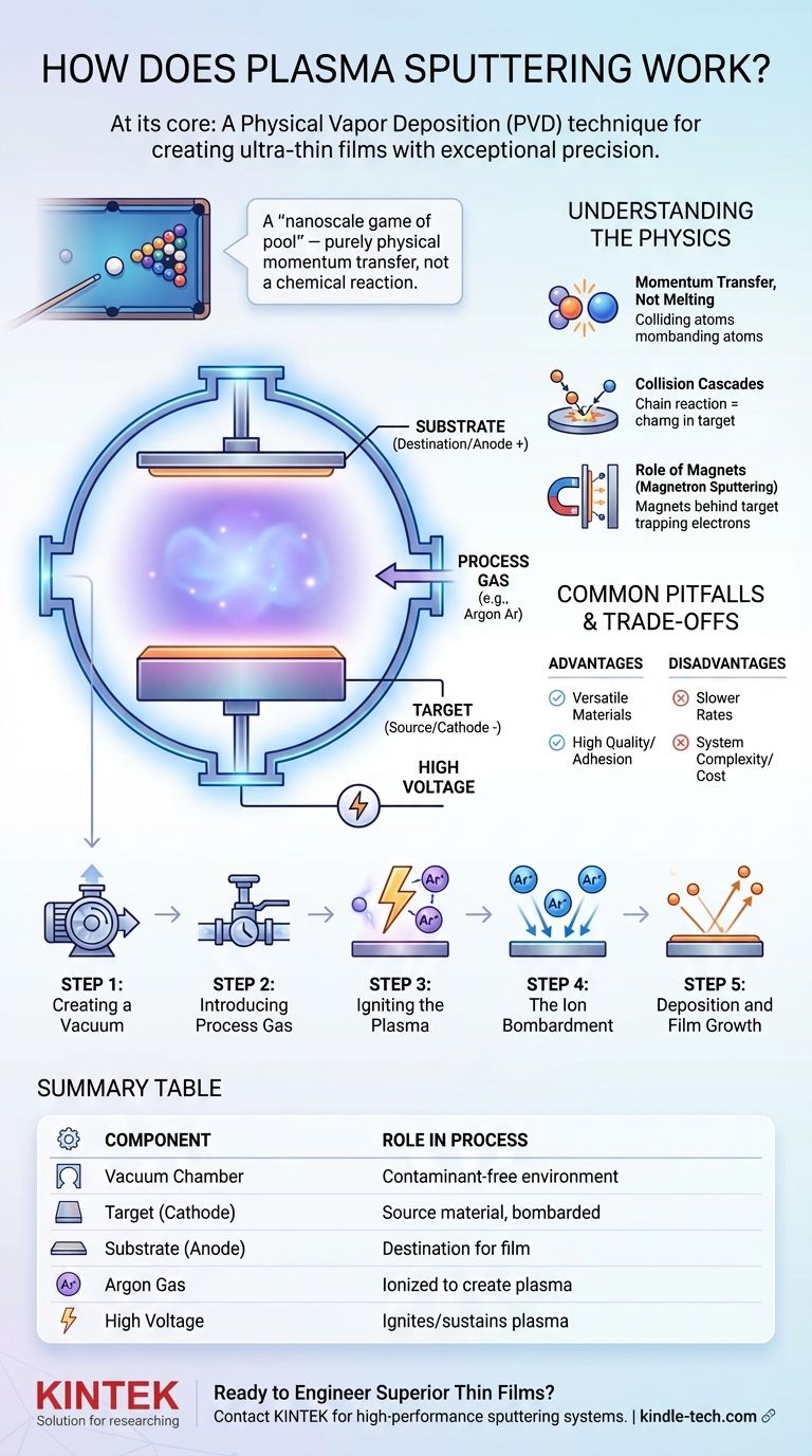
At its core, plasma sputtering is a physical vapor deposition (PVD) technique used to create ultra-thin films of material with exceptional precision. The process takes place in a vacuum and uses an energized plasma to bombard a source material, called a target. This bombardment physically knocks atoms off the target, which then travel and deposit onto a substrate, forming a uniform coating one atom at a time.
Sputtering is not a chemical reaction or a melting process. It is a purely physical mechanism of momentum transfer, best visualized as a nanoscale game of pool where energetic ions act as cue balls to eject atoms from a target material.
The Core Components of a Sputtering System
To understand how sputtering works, we must first identify the key players inside the vacuum chamber.
The Vacuum Chamber
The entire process occurs within a sealed chamber from which nearly all air has been removed. This vacuum is critical to prevent sputtered atoms from colliding with air molecules and to avoid contamination of the final film.
The Target Material (The Source)
This is a block of the pure material you wish to deposit as a thin film. It is connected to a negative voltage source, making it the cathode.
The Substrate (The Destination)
This is the object to be coated, such as a silicon wafer, glass pane, or medical implant. It is positioned to face the target and often acts as the anode in the electrical circuit.
The Process Gas (The "Ammunition")
An inert gas, most commonly Argon (Ar), is introduced into the vacuum chamber in small, controlled amounts. This gas is not part of the final film; its atoms are used as the projectiles for bombardment.
The Sputtering Process, Step-by-Step
The deposition of a thin film via sputtering follows a precise sequence of events.
Step 1: Creating a Vacuum
The chamber is sealed and pumps remove ambient air. This ensures the path from the target to the substrate is clear and that the resulting film remains uncontaminated.
Step 2: Introducing the Process Gas
A small amount of Argon gas is bled into the chamber. The pressure is low but sufficient to create the medium for the plasma.
Step 3: Igniting the Plasma
A high voltage is applied to the target material (the cathode). This powerful electric field rips electrons from the Argon atoms, creating a mixture of positively charged Argon ions (Ar+) and free electrons. This energized, ionized gas is the plasma.
Step 4: The Ion Bombardment
The positively charged Argon ions are forcefully accelerated by the electric field toward the negatively charged target. They collide with the target surface with tremendous kinetic energy.
Step 5: Deposition and Film Growth
This high-energy impact transfers momentum to the atoms of the target material, knocking them loose. These ejected atoms travel through the vacuum in a straight line and land on the substrate, where they condense and build up to form a thin, highly uniform film.
Understanding the Underlying Physics
The effectiveness of sputtering is governed by fundamental physical principles, not chemical reactions.
Momentum Transfer, Not Melting
The process is entirely mechanical at the atomic level. The Argon ions have enough energy to break the atomic bonds holding the target atoms in place, but not enough to melt the bulk material.
The Role of Collision Cascades
When an energetic ion strikes the target, it sets off a chain reaction. The ion collides with a target atom, which then collides with other target atoms in a collision cascade. When this cascade reaches the surface, atoms are ejected if the energy transferred is greater than their surface binding energy.
Key Factors Influencing Efficiency
The process is controlled by several variables. The energy of the bombarding ions, the relative masses of the ions and target atoms, and the binding energy of the target material all determine the sputter yield—the number of atoms ejected per incoming ion.
The Function of Magnets
Many modern systems are magnetron sputtering systems. Magnets are placed behind the target to create a magnetic field that traps the free electrons from the plasma near the target's surface. This dramatically increases the probability of these electrons striking and ionizing Argon atoms, creating a denser, more efficient plasma that increases deposition rates.
Common Pitfalls and Trade-offs
Sputtering is a powerful technique, but it involves clear trade-offs compared to other deposition methods.
Advantage: Material Versatility
Because it is a physical and not a thermal process, sputtering can be used to deposit almost any material, including metals, ceramics, and complex alloys, without altering their composition.
Advantage: Film Quality and Adhesion
The sputtered atoms arrive at the substrate with significant kinetic energy. This results in films that are very dense, well-adhered, and have excellent uniformity and purity.
Disadvantage: Slower Deposition Rates
Compared to thermal evaporation, sputtering is generally a slower process. This can make it less suitable for applications requiring very thick coatings on a mass-production scale.
Disadvantage: System Complexity and Cost
Sputtering systems require a high-vacuum environment, high-voltage power supplies, and precise gas flow control. This makes the equipment more complex and expensive than some alternative methods.
Applying Sputtering to Your Goal
Choosing sputtering depends entirely on the specific properties you need in your final thin film.
- If your primary focus is precision and control: Sputtering offers atomic-level control over film thickness and uniformity, making it ideal for optics and semiconductors.
- If your primary focus is film purity and density: The high-vacuum environment and energetic deposition ensure the creation of high-purity, dense films with strong adhesion.
- If your primary focus is depositing complex alloys: Sputtering transfers the target material's composition directly to the substrate, preserving the stoichiometry of complex materials.
Understanding this process of controlled, atomic-scale construction is the first step toward engineering materials with precisely tailored properties.
Summary Table:
| Key Component | Role in the Process |
|---|---|
| Vacuum Chamber | Creates a contaminant-free environment for deposition. |
| Target (Cathode) | The source material that is bombarded to release atoms. |
| Substrate (Anode) | The surface where the thin film is deposited. |
| Argon Gas | Ionized to create the plasma that bombards the target. |
| High Voltage | Ignites and sustains the plasma for the sputtering process. |
Ready to Engineer Superior Thin Films?
Plasma sputtering is key to creating high-purity, uniform coatings for demanding applications in R&D and manufacturing. KINTEK specializes in high-performance lab equipment, including sputtering systems, to meet your precise deposition needs.
Let's achieve your material science goals together. Contact our experts today to discuss your project and find the ideal solution.
Visual Guide
Related Products
- Spark Plasma Sintering Furnace SPS Furnace
- Chemical Vapor Deposition CVD Equipment System Chamber Slide PECVD Tube Furnace with Liquid Gasifier PECVD Machine
- RF PECVD System Radio Frequency Plasma-Enhanced Chemical Vapor Deposition RF PECVD
- Microwave Plasma Chemical Vapor Deposition MPCVD Machine System Reactor for Lab and Diamond Growth
- 915MHz MPCVD Diamond Machine Microwave Plasma Chemical Vapor Deposition System Reactor
People Also Ask
- What technical advantages does a Spark Plasma Sintering (SPS) furnace offer for LZP ceramics? Enhance Ionic Conductivity
- What are the advantages of CAMI/SPS for W-Cu composite preparation? Reduce cycles from hours to seconds.
- What are the fundamentals of spark plasma sintering process? Unlock Rapid, High-Performance Material Consolidation
- What is the difference between spark plasma sintering and flash sintering? A Guide to Advanced Sintering Methods
- Why are Spark Plasma Sintering (SPS) furnaces or hot presses utilized in the preparation of Li3PS4 solid electrolytes?


