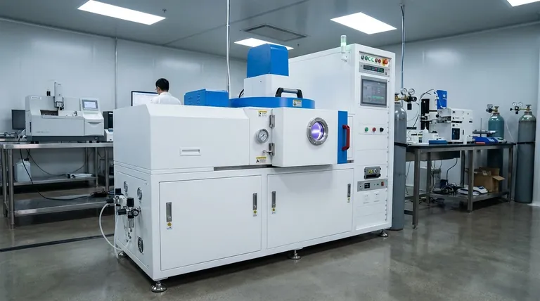
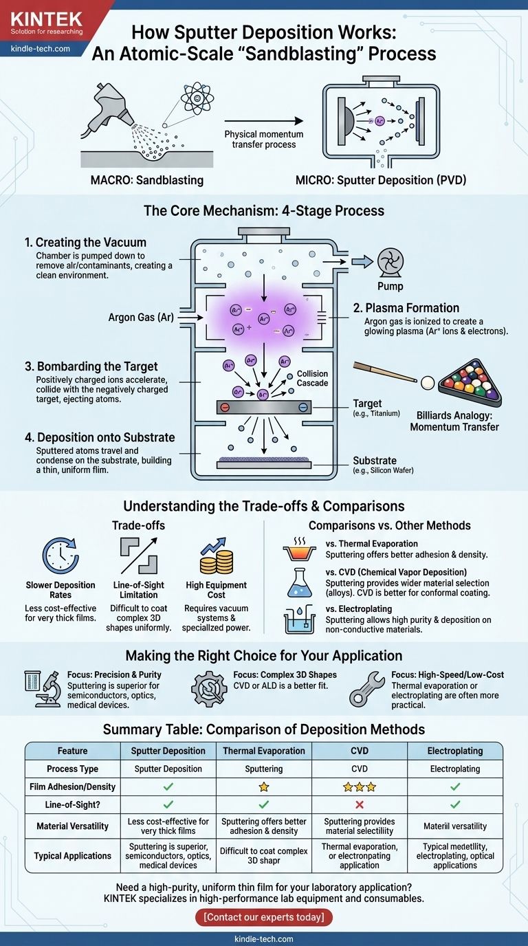
At its core, sputter deposition is an atomic-scale "sandblasting" process. It is a physical vapor deposition (PVD) method where a target material is bombarded with energetic ions inside a vacuum. This bombardment physically knocks atoms off the target, which then travel and deposit onto a substrate, forming an extremely thin and uniform film.
Sputter deposition is not a chemical reaction but a physical momentum transfer process. Think of it as using high-speed atomic "cue balls" (ions) to break off atoms from a "rack" (the target material), which then coat your component (the substrate) with remarkable precision and control.
The Core Mechanism of Sputter Deposition
To understand how sputtering works, it's best to break it down into four distinct stages that occur inside a specialized vacuum chamber.
Step 1: Creating the Vacuum Environment
First, the chamber containing the substrate and target material is pumped down to a very low pressure. This vacuum is critical because it removes air and other particles that could contaminate the film or interfere with the process.
A clean environment ensures that the sputtered atoms can travel from the target to the substrate without colliding with unwanted gas molecules.
Step 2: Plasma Formation
An inert gas, most commonly Argon, is then introduced into the chamber at a controlled low pressure. A strong electric field is applied, which strips electrons from the Argon atoms.
This process of ionization creates a plasma, an electrically charged gas consisting of positive Argon ions and free electrons. This glowing plasma is the source of the energetic particles needed for the process.
Step 3: Bombarding the Target
The target, which is the source material for the film (e.g., a disk of titanium or silicon), is given a negative electrical charge. This causes the positively charged Argon ions from the plasma to accelerate and violently collide with the target surface.
Each impact sets off a collision cascade within the target material, transferring momentum like a microscopic billiards break. This collision ejects, or "sputters," individual atoms from the target surface.
Step 4: Deposition onto the Substrate
The sputtered atoms are ejected from the target with significant kinetic energy. They travel through the low-pressure vacuum chamber until they strike a surface.
When these atoms hit the substrate (such as a silicon wafer or an optical lens), they condense and stick, gradually building up a thin, dense, and highly adherent film. The process is continued until the desired film thickness is achieved.
Understanding the Trade-offs
Sputtering is a powerful technique, but it's not the universal solution for all coating needs. Understanding its limitations is key to using it effectively.
Slower Deposition Rates
Compared to other methods like thermal evaporation or electroplating, sputtering can be a relatively slow process. This can make it less cost-effective for applications requiring very thick films or high-throughput manufacturing.
Line-of-Sight Limitation
Sputtering is fundamentally a line-of-sight process. Atoms travel in a straight line from the target to the substrate. This makes it challenging to uniformly coat complex, three-dimensional shapes or the inside of a narrow structure.
High Equipment Cost
The need for high-vacuum systems, specialized power supplies, and high-purity target materials makes the initial investment in sputtering equipment significantly higher than for simpler methods like chemical plating.
How Sputtering Compares to Other Methods
To truly understand sputtering, it helps to contrast it with other common deposition techniques.
vs. Thermal Evaporation
Thermal evaporation is another PVD method, but instead of using kinetic impact, it simply heats the source material until it evaporates. Sputtering generally produces films with better adhesion and density because the sputtered atoms arrive at the substrate with much higher energy.
vs. Chemical Vapor Deposition (CVD)
CVD uses chemical precursor gases that react on the substrate surface to form the film. Unlike the physical process of sputtering, CVD is not line-of-sight and can create highly conformal coatings on complex shapes. However, sputtering offers a wider selection of materials, including alloys and compounds that are difficult to create with chemical reactions.
vs. Electroplating
Electroplating is a chemical process that occurs in a liquid bath. It is often faster and cheaper for depositing thick metal films on conductive parts. Sputtering provides far greater purity, precision, and the ability to deposit on non-conductive materials like glass and plastics.
Making the Right Choice for Your Application
Selecting the correct deposition method depends entirely on your project's technical and commercial goals.
- If your primary focus is precision, purity, and film quality: Sputtering is the superior choice for demanding applications like semiconductors, optical filters, and medical devices.
- If your primary focus is coating a complex 3D shape uniformly: A chemical process like CVD or Atomic Layer Deposition (ALD) is a better fit.
- If your primary focus is high-speed, low-cost coating of simple metal parts: Thermal evaporation or electroplating are often more practical and economical alternatives.
By understanding the physical principles behind sputter deposition, you can confidently determine when to leverage its unique advantages for your specific goal.
Summary Table:
| Feature | Sputter Deposition | Thermal Evaporation | Chemical Vapor Deposition (CVD) | Electroplating |
|---|---|---|---|---|
| Process Type | Physical (PVD) | Physical (PVD) | Chemical | Chemical (Liquid) |
| Film Adhesion/Density | Excellent | Good | Good | Fair |
| Line-of-Sight? | Yes | Yes | No | No (for conductive parts) |
| Material Versatility | High (metals, alloys, ceramics) | Moderate | Limited by chemical precursors | Limited to conductive materials |
| Typical Applications | Semiconductors, optics, medical devices | Simple metallization | Complex 3D part coating | Decorative/protective metal coatings |
Need a high-purity, uniform thin film for your laboratory application?
Sputter deposition is ideal for demanding sectors like semiconductor manufacturing, medical device coating, and advanced optics. KINTEK specializes in providing high-performance lab equipment and consumables to meet your precise coating requirements.
Contact our experts today to discuss how our sputtering solutions can enhance your research and development process.
Visual Guide
Related Products
- Chemical Vapor Deposition CVD Equipment System Chamber Slide PECVD Tube Furnace with Liquid Gasifier PECVD Machine
- HFCVD Machine System Equipment for Drawing Die Nano-Diamond Coating
- RF PECVD System Radio Frequency Plasma-Enhanced Chemical Vapor Deposition RF PECVD
- 915MHz MPCVD Diamond Machine Microwave Plasma Chemical Vapor Deposition System Reactor
- Customer Made Versatile CVD Tube Furnace Chemical Vapor Deposition Chamber System Equipment
People Also Ask
- What happens during deposition chemistry? Building Thin Films from Gaseous Precursors
- What are the advantages of chemical vapor deposition? Achieve Superior Thin Films for Your Lab
- How expensive is chemical vapor deposition? Understanding the True Cost of High-Performance Coating
- Why is Chemical Vapor Deposition (CVD) equipment uniquely suited for constructing hierarchical superhydrophobic structures?
- What are the processes of vapor phase deposition? Understand CVD vs. PVD for Superior Thin Films


