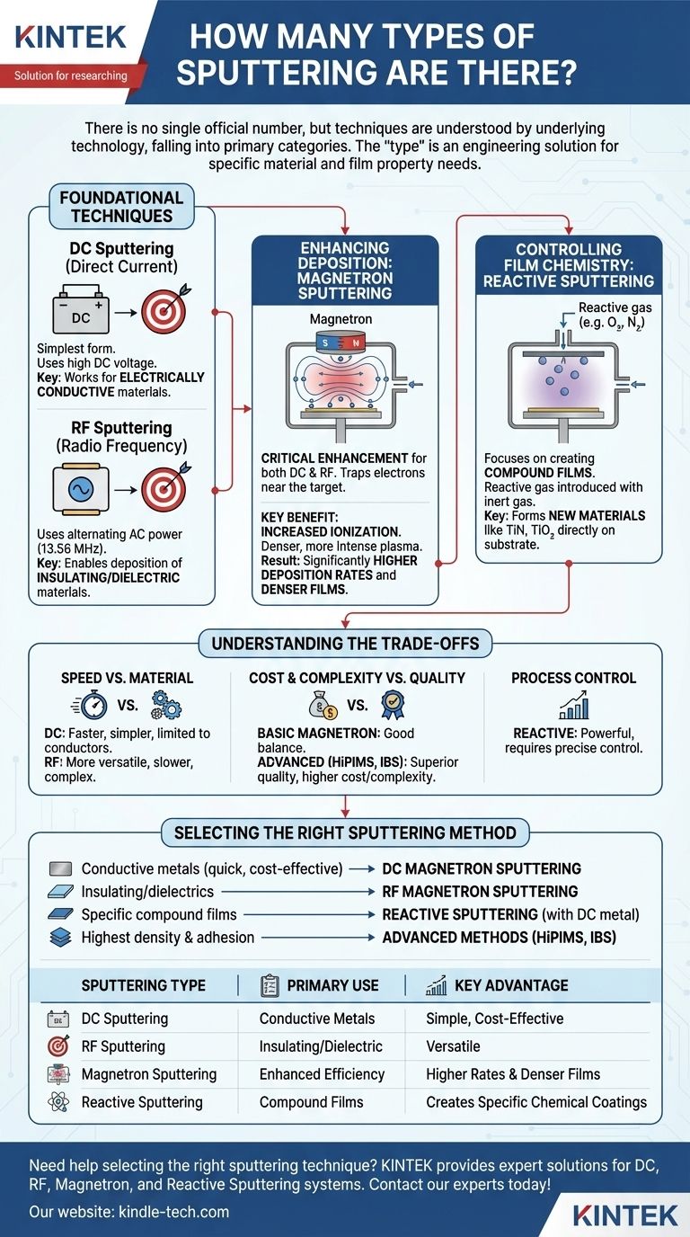
While there is no single official number, sputtering techniques are best understood by their underlying technology, which falls into a few primary categories. The main types are DC Sputtering, RF Sputtering, Magnetron Sputtering (which enhances DC and RF), and Reactive Sputtering. More advanced variations like HiPIMS and Ion Beam Sputtering exist for highly specialized applications.
The "type" of sputtering is not just a label; it represents a specific engineering solution designed to overcome a fundamental limitation, such as the inability to deposit insulating materials or the need for faster deposition rates. The right choice is determined entirely by the material you need to deposit and the film properties you need to achieve.
Foundational Sputtering Techniques
At its core, sputtering uses a plasma to bombard a source material (the "target"), knocking atoms loose that then deposit as a thin film onto a substrate. The two foundational methods are defined by the type of electrical power used to generate that plasma.
DC Sputtering: The Original Method
Direct Current (DC) sputtering is the simplest form. A high DC voltage is applied to the target in a vacuum chamber filled with an inert gas like argon.
This creates a plasma, and the positive argon ions are accelerated into the negatively charged target, ejecting atoms. Its primary limitation is that it only works for electrically conductive target materials.
RF Sputtering: The Solution for Insulators
When trying to sputter an insulating (dielectric) material with a DC source, positive charge builds up on the target surface, effectively stopping the process.
Radio Frequency (RF) sputtering solves this by using an alternating AC power source (typically 13.56 MHz). The rapid switching of the electric field allows the target to self-neutralize on each cycle, enabling the consistent sputtering of insulating and dielectric materials like oxides and ceramics.
Enhancing Deposition: The Role of Magnetrons
The foundational DC and RF methods are effective but relatively slow. Magnetron sputtering is not a separate type but rather a critical enhancement that dramatically improves the efficiency of both.
How Magnetron Sputtering Works
In magnetron sputtering, a strong magnetic field is configured behind the sputtering target. This field traps the free electrons from the plasma, confining them to a region directly in front of the target surface.
The Key Benefit: Increased Ionization
These trapped, spiraling electrons have a much longer path length, greatly increasing the probability that they will collide with and ionize neutral argon atoms.
This process creates a much denser, more intense plasma concentrated near the target, all without needing to increase the gas pressure.
The Result: Faster and Denser Films
A denser plasma means more ions are available to bombard the target. This results in significantly higher deposition rates and often leads to higher-quality, denser films being deposited on the substrate. Today, most modern systems are magnetron-based, referred to as DC Magnetron Sputtering or RF Magnetron Sputtering.
Controlling Film Chemistry: Reactive Sputtering
This technique focuses on creating compound films, not just depositing a pure material. It can be combined with DC or RF magnetron sputtering.
Sputtering in a Reactive Atmosphere
In reactive sputtering, a small amount of a reactive gas, such as oxygen or nitrogen, is intentionally introduced into the vacuum chamber along with the inert argon gas.
Creating Compound Films
As atoms are sputtered from the metallic target (e.g., titanium), they travel toward the substrate and react with this gas. This allows you to form new compound films directly on the substrate, such as titanium nitride (TiN) or titanium dioxide (TiO2).
Understanding the Trade-offs
Choosing a sputtering technique involves balancing performance, cost, and material compatibility. There is no single "best" method.
Speed vs. Material Compatibility
The most fundamental trade-off is between DC and RF sputtering. DC is faster and simpler but is strictly limited to conductive materials. RF is more versatile, capable of depositing any material, but is generally slower and requires more complex and expensive power supplies.
Cost & Complexity vs. Film Quality
Basic magnetron sputtering offers an excellent balance of speed and quality for most applications. However, advanced methods like High-Power Impulse Magnetron Sputtering (HiPIMS) or Ion Beam Sputtering (IBS) offer superior film density, adhesion, and purity at the cost of significantly higher equipment complexity and expense.
Process Control
Reactive sputtering is incredibly powerful for creating hard or optical coatings, but it introduces a major process control challenge. Balancing the reaction rate to avoid poisoning the target while ensuring a fully reacted film requires highly precise gas flow and power management.
Selecting the Right Sputtering Method
Your choice should be guided directly by your end goal for the thin film.
- If your primary focus is depositing conductive metals quickly and cost-effectively: Your starting point is DC Magnetron Sputtering.
- If your primary focus is depositing insulating or dielectric materials like oxides or ceramics: You require RF Magnetron Sputtering.
- If your primary focus is creating specific compound films like nitrides or carbides: You will need to use Reactive Sputtering, typically with a DC-powered metallic target.
- If your primary focus is achieving the highest possible film density and adhesion for critical applications: You should investigate advanced methods like HiPIMS or Ion Beam Sputtering.
Understanding these core methods and their intended applications is the first step toward achieving your specific thin-film deposition goals.
Summary Table:
| Sputtering Type | Primary Use | Key Advantage |
|---|---|---|
| DC Sputtering | Conductive Metals | Simple, Cost-Effective |
| RF Sputtering | Insulating/Dielectric Materials | Versatile for Non-Conductors |
| Magnetron Sputtering | Enhanced DC/RF Efficiency | Higher Deposition Rates & Denser Films |
| Reactive Sputtering | Compound Films (e.g., Nitrides, Oxides) | Creates Specific Chemical Coatings |
Need help selecting the right sputtering technique for your lab's thin-film deposition? KINTEK specializes in lab equipment and consumables, providing expert solutions for DC, RF, Magnetron, and Reactive Sputtering systems. We'll help you achieve precise film properties, improve deposition efficiency, and ensure material compatibility. Contact our experts today to discuss your specific application and get a tailored recommendation!
Visual Guide
Related Products
- Chemical Vapor Deposition CVD Equipment System Chamber Slide PECVD Tube Furnace with Liquid Gasifier PECVD Machine
- Twin Screw Extruder Plastic Granulation Machine
- Single Punch Manual Tablet Press Machine TDP Tablet Punching Machine
- Three-dimensional electromagnetic sieving instrument
- HFCVD Machine System Equipment for Drawing Die Nano-Diamond Coating
People Also Ask
- How expensive is chemical vapor deposition? Understanding the True Cost of High-Performance Coating
- What types of substrates are used in CVD to facilitate graphene films? Optimize Graphene Growth with the Right Catalyst
- What are the processes of vapor phase deposition? Understand CVD vs. PVD for Superior Thin Films
- What are the advantages of chemical vapor deposition? Achieve Superior Thin Films for Your Lab
- What is plasma enhanced chemical vapor deposition PECVD equipment? A Guide to Low-Temperature Thin Film Deposition