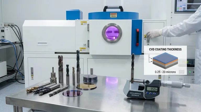
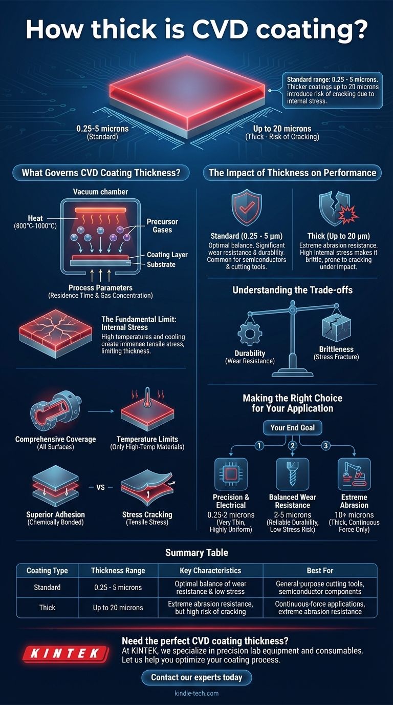
In most industrial applications, a Chemical Vapor Deposition (CVD) coating has a thickness between 0.25 and 5 microns. While this is the standard range, some specialized applications may use thicker coatings of up to 20 microns. However, this increased thickness introduces significant trade-offs, particularly the risk of cracking due to internal stress.
The thickness of a CVD coating is not an accident of the process but a critical engineering decision. The choice balances the need for wear resistance against the inherent physical stress that limits how thick the coating can be before its structural integrity is compromised.
What Governs CVD Coating Thickness?
To understand the implications of thickness, you must first understand how it is controlled and why it is naturally limited. The deposition process itself contains the key.
The Core Deposition Process
Chemical Vapor Deposition involves heating a substrate (the part being coated) in a vacuum chamber. Volatile precursor gases are introduced, which react and decompose on the hot surface, creating a new, thin layer of material that is chemically bonded to the part.
Controlling Thickness with Process Parameters
Engineers have precise control over the final film thickness. It is not a random outcome. The thickness is primarily determined by adjusting process variables like the residence time—how long the part is exposed to the precursor gases—and the concentration of those gases.
The Fundamental Limit: Internal Stress
The primary factor limiting CVD thickness is internal stress. The process occurs at very high temperatures, often between 800°C and 1000°C. As the part and its new coating cool down, differences in their thermal expansion rates create immense tensile stress within the coating layer. The thicker the coating, the greater this stored stress becomes.
The Impact of Thickness on Performance
The thickness you target is directly related to the performance you need and the risks you are willing to accept. The choice generally falls into two categories.
Standard Coatings (0.25 - 5 microns)
This range represents the optimal balance for most applications. It provides a significant increase in wear resistance and durability without accumulating enough internal stress to risk spontaneous cracking. These coatings are common on semiconductor components and general-purpose cutting tools.
Thick Coatings (up to 20 microns)
A thicker coating is sometimes used for applications demanding extreme abrasion resistance. However, the high internal stress makes the coating more brittle. These thick films are prone to developing fine cracks, which can spread under impact or fluctuating loads, causing the coating to peel.
This brittleness makes thick CVD coatings suitable for processes with continuous, uniform force, but a poor choice for interrupted cutting operations like milling, where repeated impacts can easily cause the coating to fail.
Understanding the Trade-offs
Choosing a CVD coating requires a clear-eyed assessment of its advantages and limitations. The process is not a universal solution, and thickness is at the heart of its central trade-off.
Durability vs. Brittleness
The core conflict is between wear resistance and integrity. A thicker coating provides more sacrificial material to wear away, but the accompanying internal stress makes it brittle and susceptible to fracture under impact.
Comprehensive Coverage vs. Temperature Limits
Unlike line-of-sight processes (like PVD), CVD gases can coat all surfaces of a complex part, including internal threads and blind holes. However, the extreme heat required limits the substrate materials that can be used. Only materials with high temperature resistance, such as cemented carbides, can be coated without being damaged.
Superior Adhesion vs. Stress Cracking
The chemical reaction at the heart of CVD creates a powerful, chemically-bonded layer with superior adhesion to the substrate. This is a primary advantage of the process. Yet, this is directly opposed by the tensile stress that tries to pull the coating apart as it cools.
Making the Right Choice for Your Application
The ideal coating thickness is dictated entirely by your end goal and the limitations of your base material.
- If your primary focus is precision and electrical properties (e.g., semiconductors): You will need a very thin and highly uniform coating, often in the 0.25 to 2-micron range.
- If your primary focus is balanced wear resistance on complex tools: The standard range of 2 to 5 microns provides a reliable profile of durability without excessive risk of stress failure.
- If your primary focus is extreme abrasion resistance in a continuous-force application: Thicker coatings (10+ microns) can be considered, but you must ensure your base material can survive the process heat and that the application is free from impacts.
Ultimately, selecting the right CVD coating thickness requires a clear understanding of your material's limits and your application's specific mechanical demands.
Summary Table:
| Coating Type | Thickness Range | Key Characteristics | Best For |
|---|---|---|---|
| Standard | 0.25 - 5 microns | Optimal balance of wear resistance & low stress | General-purpose cutting tools, semiconductor components |
| Thick | Up to 20 microns | Extreme abrasion resistance, but high risk of cracking | Continuous-force applications, extreme abrasion resistance |
Need the perfect CVD coating thickness for your tools?
At KINTEK, we specialize in precision lab equipment and consumables for advanced material processing. Our expertise ensures you achieve the ideal balance of wear resistance and structural integrity for your specific application—whether it's semiconductor components or industrial cutting tools.
Let us help you optimize your coating process for maximum durability and performance. Contact our experts today for a tailored solution!
Visual Guide
Related Products
- Custom CVD Diamond Coating for Lab Applications
- HFCVD Machine System Equipment for Drawing Die Nano-Diamond Coating
- Laboratory CVD Boron Doped Diamond Materials
- CVD Diamond for Thermal Management Applications
- CVD Diamond Dressing Tools for Precision Applications
People Also Ask
- Can you coat something in diamond? Unlock Unmatched Hardness and Thermal Conductivity
- What are the advantages of CVD coating? Superior Hardness and Uniformity for Demanding Applications
- What are the different CVD coating? A Guide to Thermal CVD, PECVD, and Specialized Methods
- What is CVD coated? A Guide to Superior Wear Resistance for Complex Parts
- What is CVD coating? Transform Your Material's Surface for Maximum Performance


