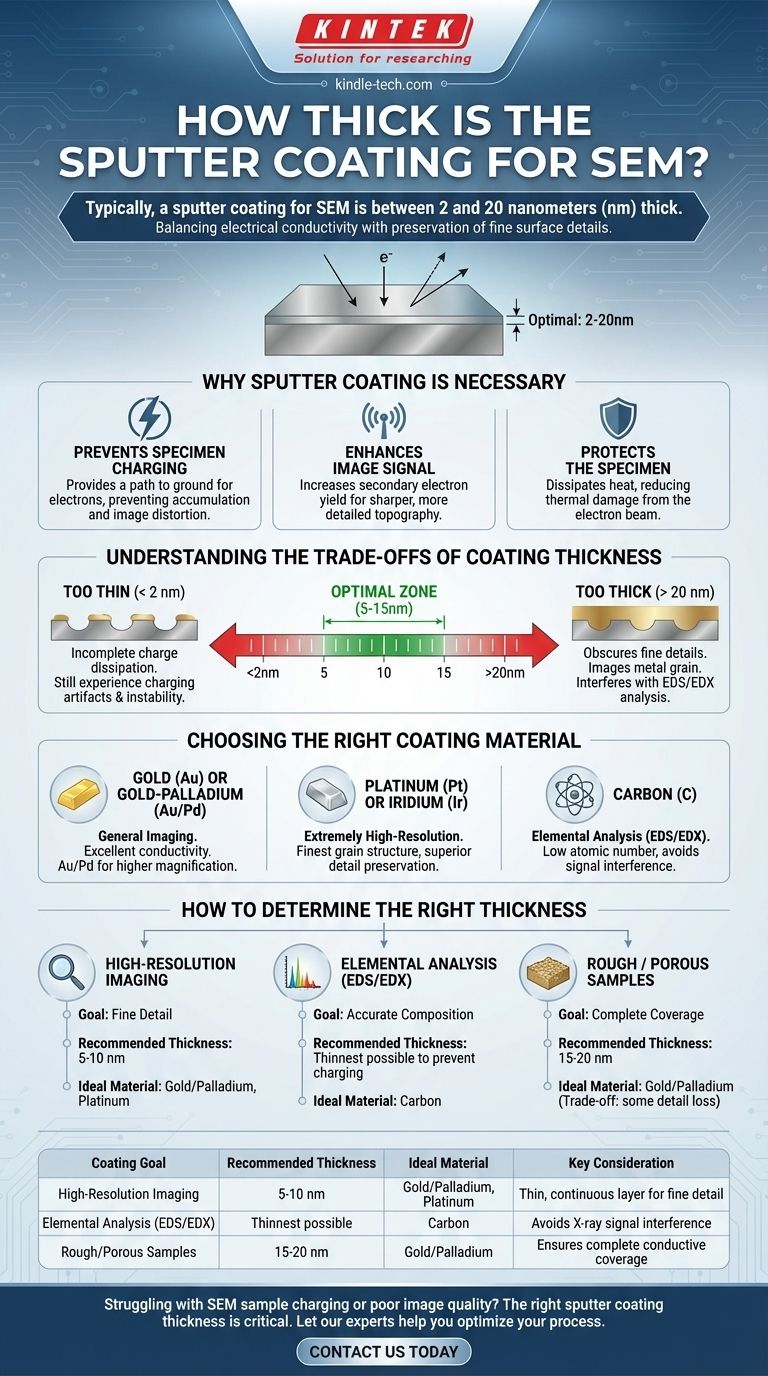
Typically, a sputter coating for SEM is between 2 and 20 nanometers (nm) thick. This ultra-thin, electrically conductive layer is applied to non-conductive samples to prevent imaging artifacts and improve signal quality. The goal is to create a uniform metallic film that is thick enough to conduct away electrical charge but thin enough that it doesn't obscure the specimen's true surface topography.
The core challenge of sputter coating is not simply to apply a coating, but to achieve a precise thickness that balances electrical conductivity with the preservation of fine surface details. The ideal thickness is entirely dependent on your specimen and your analytical goals.

Why Sputter Coating is Necessary
Before discussing thickness, it is essential to understand why this step is critical for imaging many types of samples in a Scanning Electron Microscope (SEM). The process addresses several fundamental problems that arise when a high-energy electron beam interacts with a non-conductive surface.
Preventing Specimen Charging
The primary purpose of a sputter coat is to provide a path to ground for the electrons striking the sample. Without it, electrons accumulate on a non-conductive surface, creating a negative charge.
This localized charging deflects the incoming electron beam, leading to severe image distortions, unnatural brightness, and drifting, which make it impossible to acquire a clear and stable image.
Enhancing Image Signal
A good sputter coating material, like gold or platinum, has a high secondary electron (SE) yield. Secondary electrons are the primary signal used for generating high-resolution images of surface topography.
By coating the sample, you significantly increase the number of secondary electrons emitted from the surface. This improves the signal-to-noise ratio, resulting in a sharper, more detailed image.
Protecting the Specimen
The focused electron beam deposits a significant amount of energy into a small area, which can cause thermal damage, especially to delicate biological or polymeric samples.
A conductive metal coating helps dissipate this heat away from the analysis area, reducing beam damage and preserving the sample's integrity during observation.
Understanding the Trade-offs of Coating Thickness
Choosing the right thickness is a critical decision that directly impacts the quality of your results. There are clear disadvantages to using a coating that is either too thin or too thick.
The Problem with a Coating That's Too Thin (< 2 nm)
A coating that is too thin will often be discontinuous. Instead of forming a uniform film, the metal deposits as isolated islands on the specimen surface.
These islands do not create a complete conductive path to ground, resulting in incomplete charge dissipation. You will likely still experience charging artifacts and image instability.
The Problem with a Coating That's Too Thick (> 20 nm)
A thick coating begins to obscure the very features you are trying to observe. The fine, nanoscale details of your sample's surface will be buried under the metallic layer.
Furthermore, the coating itself has a grain structure. At high magnifications, a thick coating can cause you to image the grain of the metal coating instead of your sample's actual surface.
Finally, for elemental analysis using Energy-Dispersive X-ray Spectroscopy (EDS/EDX), a thick metal coating is highly problematic. It can generate strong X-ray signals that overwhelm the signals from your actual sample or absorb the X-rays emitted from the specimen, leading to inaccurate results.
Choosing the Right Coating Material
The ideal thickness also depends on the material you choose, which should be determined by your analytical goals.
Gold (Au) or Gold-Palladium (Au/Pd)
This is the most common, all-purpose coating for general SEM imaging. Gold offers excellent conductivity and a relatively fine grain size. An Au/Pd alloy is often preferred as it produces even finer grains, making it suitable for higher magnification work.
Platinum (Pt) or Iridium (Ir)
For extremely high-resolution applications (magnifications >100,000x), platinum or iridium are superior choices. They have an exceptionally fine grain structure, which allows you to coat the sample without obscuring the finest surface details.
Carbon (C)
Carbon is the standard choice when elemental analysis (EDS/EDX) is the primary goal. Because carbon has a low atomic number, its X-ray signal does not interfere with the peaks of heavier elements in your sample, ensuring accurate compositional data. However, its conductivity is lower than that of metals.
How to Determine the Right Thickness for Your Sample
There is no single "perfect" thickness. You must adapt your coating parameters to your specific needs.
- If your primary focus is high-resolution imaging of surface topography: Aim for a thin but continuous layer (5-10 nm) of a fine-grained metal like Gold/Palladium or Platinum.
- If your primary focus is elemental analysis (EDS/EDX): Use a carbon coating to avoid signal interference. The thickness will depend on sample roughness, but you should use the thinnest layer possible that prevents charging.
- If you are working with a very rough, porous, or non-conductive sample: You may need a thicker coating (15-20 nm) to ensure complete, continuous coverage, but you must accept the trade-off of losing some fine surface detail.
Mastering sputter coating is about making an informed compromise to get the data you need.
Summary Table:
| Coating Goal | Recommended Thickness | Ideal Material | Key Consideration |
|---|---|---|---|
| High-Resolution Imaging | 5-10 nm | Gold/Palladium, Platinum | Thin, continuous layer for fine detail |
| Elemental Analysis (EDS/EDX) | Thinnest possible to prevent charging | Carbon | Avoids X-ray signal interference |
| Rough/Porous Samples | 15-20 nm | Gold/Palladium | Ensures complete conductive coverage |
Struggling with SEM sample charging or poor image quality? The right sputter coating thickness is critical for clear, stable imaging and accurate analysis. At KINTEK, we specialize in providing high-quality lab equipment and consumables, including sputter coaters and coating materials, to help you achieve perfect results for your specific samples—from delicate biological specimens to rugged materials.
Let our experts help you optimize your process. Contact us today to discuss your application and discover how KINTEK's solutions can enhance your SEM workflow!
Visual Guide
Related Products
- Infrared Transmission Coating Sapphire Sheet Substrate Window
- Electron Beam Evaporation Coating Oxygen-Free Copper Crucible and Evaporation Boat
- 400-700nm Wavelength Anti Reflective AR Coating Glass
- Custom CVD Diamond Coating for Lab Applications
- Molybdenum Tungsten Tantalum Special Shape Evaporation Boat
People Also Ask
- What is the thinnest coating? Unlocking Unique Properties at the Atomic Scale
- What are the applications of optical coating? Unlock Advanced Light Control for Your Industry
- What is optical coating used for? Control Light for Enhanced Performance in Your Applications
- Is Sputter Tint good? Premium Heat Rejection & Long-Term Durability Explained
- What do optical coatings do? Control Light for Superior Optical Performance


