In the field of thin-film deposition, sputtering is a cornerstone technique, renowned for producing high-quality, dense, and uniform coatings with exceptional adhesion. Its primary advantages lie in this precision and control, while its disadvantages center on higher system complexity, potential for substrate damage from energetic particles, and slower deposition rates for certain materials like dielectrics.
Sputtering is a high-precision physical vapor deposition (PVD) method prized for creating dense, uniform, and strongly adhered thin films. The fundamental trade-off is between this superior film quality and the higher costs, process complexity, and potential for energy-induced substrate damage compared to simpler deposition techniques.
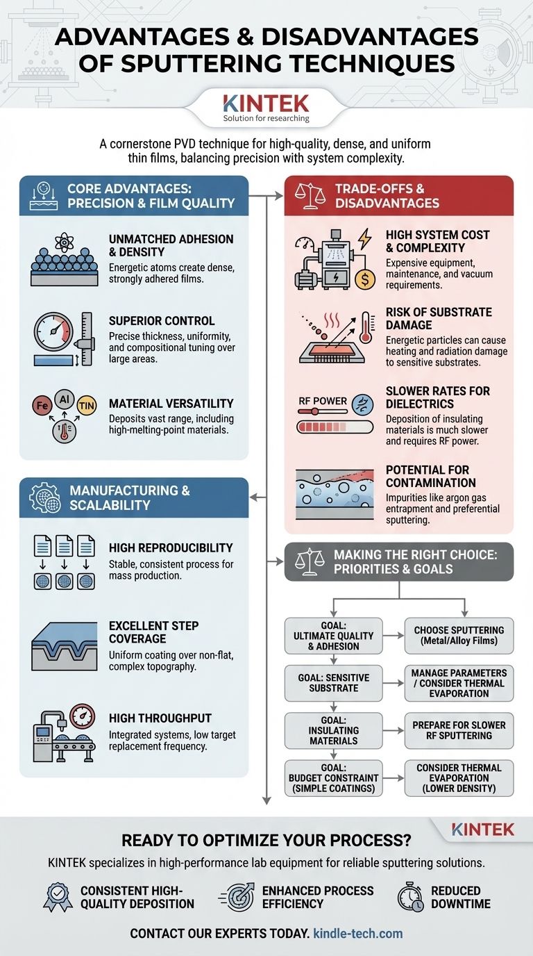
The Core Advantages: Precision and Film Quality
Sputtering's main appeal comes from its ability to create films with properties that are difficult to achieve with other methods, such as thermal evaporation.
Unmatched Film Adhesion and Density
Because sputtered atoms arrive at the substrate with significant kinetic energy, they form a denser, more tightly packed film. This energy promotes strong adhesion between the film and the substrate surface.
Superior Thickness and Compositional Control
Sputtering offers highly reproducible and precise control over film thickness and uniformity, even across large substrate areas. Techniques like magnetron sputtering allow for fine-tuning of the film's chemical composition, making it ideal for depositing complex alloys.
Versatility Across Materials
The physical nature of the process allows for the deposition of a vast range of materials, including metals, alloys, and compounds. It is particularly effective for materials with very high melting points that are impossible to deposit using thermal evaporation.
Key Benefits for Manufacturing and Scalability
Beyond film quality, sputtering is well-suited for integration into high-volume manufacturing environments.
High Reproducibility for Mass Production
The process is highly stable and controllable, with factors like power and time being easily managed. This leads to excellent reproducibility from run to run, a critical requirement for manufacturing.
Excellent Step Coverage
The sputtered material does not arrive from a single point source, resulting in better coating uniformity over complex, non-flat surfaces. This property, known as step coverage, is crucial in semiconductor fabrication.
High Throughput and Process Integration
Modern sputtering systems are designed for high throughput and can be easily integrated into automated, single-wafer processing lines. The targets (the source material being sputtered) also have a low replacement frequency, reducing machine downtime.
Understanding the Trade-offs and Disadvantages
To leverage sputtering effectively, you must be aware of its inherent complexities and limitations.
High System Cost and Complexity
Sputtering systems, with their required vacuum chambers, high-voltage power supplies, and gas handling, are significantly more complex and expensive to purchase and maintain than simpler deposition equipment.
The Risk of Substrate Heating and Damage
The energetic particles bombarding the substrate can cause unwanted heating and radiation damage. This is a major concern for temperature-sensitive substrates like plastics or certain electronic components.
Slower Deposition for Insulating Materials
While generally efficient for metals, sputtering dielectric (insulating) materials is much slower. This requires Radio Frequency (RF) power instead of Direct Current (DC), which is less efficient and introduces more heat into the system, often becoming the primary process bottleneck.
Potential for Contamination and Compositional Shifts
The process can introduce impurities, such as entrapped argon gas from the sputtering environment. Furthermore, when sputtering alloys or compounds, one element may be sputtered faster than another (preferential sputtering), altering the final composition of the film.
Making the Right Choice for Your Goal
Selecting a deposition method depends entirely on your project's priorities. Sputtering is a powerful tool, but not always the necessary one.
- If your primary focus is ultimate film quality and adhesion: Sputtering is often the superior choice, especially for dense metal or alloy films needed in demanding applications.
- If you are depositing on a temperature-sensitive substrate: You must carefully manage sputtering parameters or consider lower-energy alternatives like thermal evaporation.
- If your project involves depositing insulating materials: Be prepared for the slower rates and higher system heat load associated with RF sputtering.
- If budget is the primary constraint for simple coatings: Thermal evaporation may offer a more cost-effective solution, though likely with compromises in film density and adhesion.
By understanding these fundamental trade-offs, you can confidently select and optimize the right deposition strategy for your specific technical and commercial goals.
Summary Table:
| Aspect | Advantages | Disadvantages |
|---|---|---|
| Film Quality | High density, excellent adhesion, uniformity | Risk of substrate heating/damage |
| Process Control | Precise thickness & composition control | High system cost and complexity |
| Material Versatility | Deposits metals, alloys, high-melting-point materials | Slow deposition rates for dielectrics (insulators) |
| Manufacturing | High reproducibility, good step coverage, scalable | Potential for contamination (e.g., argon entrapment) |
Ready to Optimize Your Thin-Film Deposition Process?
Sputtering is a powerful technique, but its success depends on using the right equipment configured for your specific materials and application. KINTEK specializes in high-performance lab equipment and consumables, providing the reliable sputtering solutions your laboratory needs.
We help our customers in semiconductors, R&D, and advanced materials manufacturing achieve:
- Consistent, high-quality film deposition with excellent adhesion and uniformity.
- Enhanced process efficiency through optimized system design and support.
- Reduced downtime with durable targets and expert technical service.
Let's discuss your project requirements. Contact our experts today to find the ideal sputtering solution for your laboratory's challenges and goals.
Visual Guide
Related Products
- Spark Plasma Sintering Furnace SPS Furnace
- Vacuum Induction Melting Spinning System Arc Melting Furnace
- Chemical Vapor Deposition CVD Equipment System Chamber Slide PECVD Tube Furnace with Liquid Gasifier PECVD Machine
- Customer Made Versatile CVD Tube Furnace Chemical Vapor Deposition Chamber System Equipment
People Also Ask
- What are the fundamentals of spark plasma sintering process? Unlock Rapid, High-Performance Material Consolidation
- What is the pressure for spark plasma sintering? A Guide to Optimizing SPS Parameters
- What technical advantages does a Spark Plasma Sintering (SPS) furnace offer for LZP ceramics? Enhance Ionic Conductivity
- What is the theory of spark plasma sintering? A Guide to Rapid, Low-Temperature Densification
- What are the advantages of CAMI/SPS for W-Cu composite preparation? Reduce cycles from hours to seconds.


