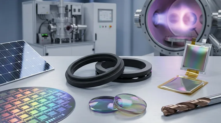
In short, chemical thin films are used in nearly every advanced industry to impart specific properties—like corrosion resistance, electrical conductivity, or optical transparency—onto the surface of a material. Their applications range from protective coatings on aerospace components and cutting tools to the functional layers in solar cells, touch screens, and semiconductor devices.
The true power of thin films is not just in providing a coating, but in creating entirely new functional surfaces. By engineering materials at the atomic scale, we can unlock unique properties that are fundamentally different from the bulk material, enabling technologies that would otherwise be impossible.
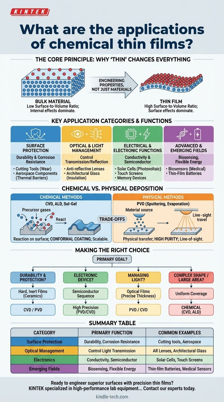
The Core Principle: Why "Thin" Changes Everything
The vast applicability of thin films stems from a single principle of physics. When a material is reduced to a layer only a few atoms or molecules thick, its fundamental properties change.
A Shift in Surface-to-Volume Ratio
In a bulk material, the vast majority of atoms are on the inside, shielded by their neighbors. In a thin film, a significant percentage of atoms are on the surface.
This high surface-to-volume ratio means that surface effects, which are negligible in bulk materials, become dominant. This allows us to engineer these surfaces for specific tasks.
Engineering Properties, Not Just Materials
We are no longer just using a material; we are designing a functional system. A thin film can be customized to be optically active, electrically conductive, exceptionally hard, or chemically inert.
This turns a simple substrate, like glass or metal, into a high-performance component with precisely the properties required for a given application.
Key Application Categories and Their Functions
Rather than a simple list, it's more useful to think of applications in terms of the function the thin film provides.
Surface Protection and Durability
This is one of the most common uses. Thin films act as a shield between a component and a hostile environment.
Ceramic thin films, for example, are prized for their high hardness and chemical inertness. They are used as protective coatings to prevent corrosion, oxidation, and wear on everything from bathroom fittings to industrial cutting tools, often extending the life of the tool by orders of magnitude. In aerospace, they serve as critical thermal barriers.
Optical and Light Management
Thin films can be engineered to control light with incredible precision. This is achieved by creating single or multiple layers that reflect, absorb, or transmit specific wavelengths.
Applications include anti-reflection coatings on ophthalmic lenses, mirrors in reflector lamps, head-up displays in cars, and advanced architectural glass that provides thermal insulation by reflecting infrared radiation.
Electrical and Electronic Functions
Modern electronics would not exist without thin films. Layers of conductive, insulating, and semiconducting materials are deposited to build complex circuits on a microscopic scale.
This is the basis for semiconductor devices, thin-film photovoltaic cells (solar panels), computer memory, and the transparent conductive layers used in touch-panel displays.
Advanced and Emerging Fields
The versatility of thin films makes them central to next-generation technology.
Applications are rapidly growing in areas like biosensors, where a film is designed to react to specific biological molecules, and thin-film batteries, which promise lighter and more flexible energy storage solutions.
Understanding the Trade-offs: Chemical vs. Physical Deposition
The term "chemical thin film" typically refers to the manufacturing process. The choice of process is a critical engineering decision with significant trade-offs.
What Defines a "Chemical" Method?
Deposition methods are broadly split into two families: Chemical and Physical.
Chemical methods involve a chemical reaction on the substrate's surface, which forms the film. Key processes include Chemical Vapor Deposition (CVD), Atomic Layer Deposition (ALD), and Sol-Gel coating.
The Advantage of Chemical Methods
Chemical deposition processes are often superior at creating a uniform, continuous film over complex, non-flat surfaces.
Because the film "grows" on the surface via a reaction, it can conform to intricate shapes, which is a major advantage over line-of-sight physical methods. They can also be highly scalable for large-volume manufacturing.
When to Consider Physical Methods
Physical Vapor Deposition (PVD) methods, like sputtering or thermal evaporation, physically transfer material onto the substrate in a vacuum.
These methods can offer extremely high purity and are often preferred for high-precision applications, such as certain optical coatings or advanced semiconductors, where even minuscule impurities from a chemical precursor are unacceptable.
Making the Right Choice for Your Application
The optimal thin film strategy depends entirely on your primary goal.
- If your primary focus is durability and protection: Use hard, inert films like ceramics, often applied via chemical or physical vapor deposition to create a robust barrier against wear and corrosion.
- If your primary focus is an electronic device: Use a sequence of semiconductor, conductive, and insulating films deposited with high precision to build the functional electronic architecture.
- If your primary focus is managing light: Use single or multi-layer optical films whose thickness is precisely controlled to interfere with specific wavelengths for anti-reflection, filtering, or mirroring.
- If your primary focus is coating a complex shape or large area: Chemical deposition methods like CVD are often the most effective choice for ensuring complete and uniform coverage.
By understanding these core functions, you can select and specify thin films not as a simple coating, but as an integrated design element that unlocks new performance.
Summary Table:
| Application Category | Primary Function | Common Examples |
|---|---|---|
| Surface Protection | Durability & Corrosion Resistance | Cutting tools, aerospace components |
| Optical Management | Control Light Transmission/Reflection | Anti-reflective lenses, architectural glass |
| Electronics | Conductivity & Semiconductor Functions | Solar cells, touch screens, memory devices |
| Emerging Fields | Biosensing, Flexible Energy Storage | Thin-film batteries, medical sensors |
Ready to engineer superior surfaces with precision thin films? KINTEK specializes in high-performance lab equipment and consumables for thin film deposition, including Chemical Vapor Deposition (CVD) and Atomic Layer Deposition (ALD) systems. Whether you're developing durable coatings, advanced electronics, or optical components, our solutions help you achieve uniform, reliable results—even on complex shapes. Contact our experts today to discuss how we can support your laboratory's thin film innovation.
Visual Guide
Related Products
- Custom CVD Diamond Coating for Lab Applications
- Electron Beam Evaporation Coating Oxygen-Free Copper Crucible and Evaporation Boat
- Laboratory CVD Boron Doped Diamond Materials
- HFCVD Machine System Equipment for Drawing Die Nano-Diamond Coating
- CVD Diamond Cutting Tool Blanks for Precision Machining
People Also Ask
- What are the advantages of CVD coating? Superior Hardness and Uniformity for Demanding Applications
- What is CVD diamond coating? Grow a Super-Hard, High-Performance Diamond Layer
- What are the types of CVD coating? A Guide to Choosing the Right Process
- What is CVD coating used for? Hardening Tools & Building Semiconductors for Industry
- What are the different CVD coating? A Guide to Thermal CVD, PECVD, and Specialized Methods


