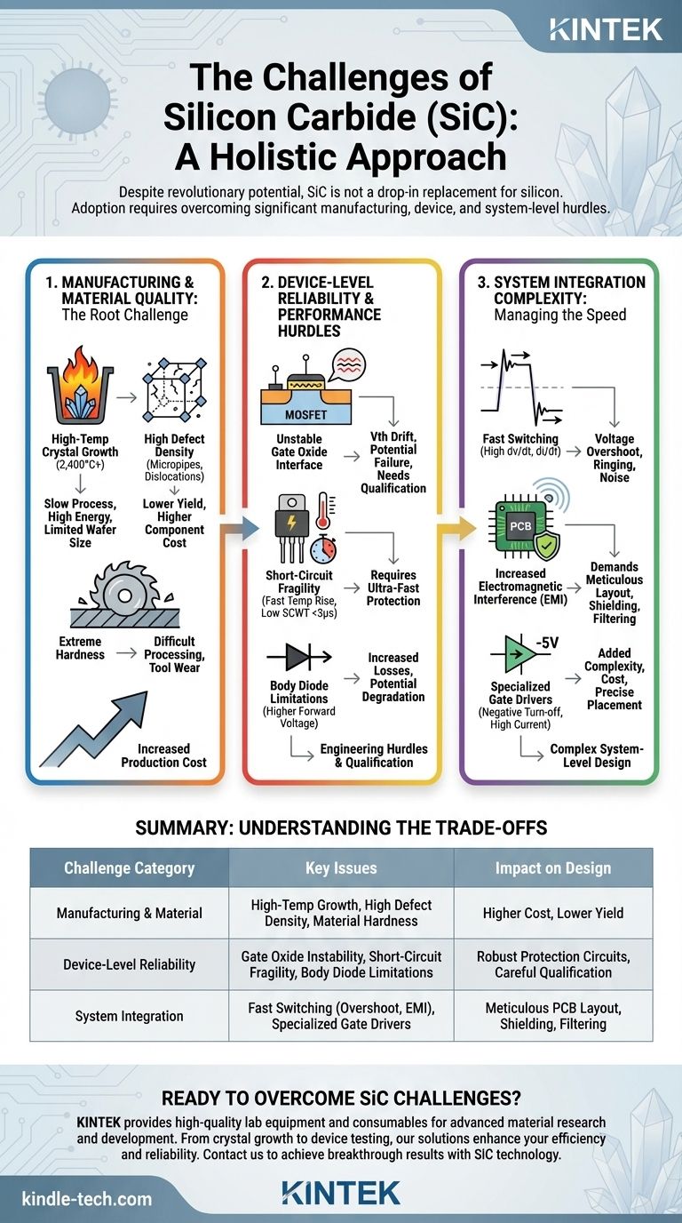
Despite its revolutionary potential, silicon carbide (SiC) is not a simple drop-in replacement for silicon. The primary challenges slowing its universal adoption stem from fundamental difficulties in manufacturing the raw material, which leads to higher costs and defect rates. At the device level, long-term reliability of the gate oxide and fragility under short-circuit conditions present significant engineering hurdles, while its fast switching speeds create complex system-level integration problems like electromagnetic interference (EMI).
While SiC enables unprecedented gains in efficiency and power density, its adoption requires a holistic engineering approach. The core challenges are rooted in its material immaturity compared to silicon, demanding that designers fundamentally rethink everything from circuit layout and thermal management to protection schemes.
The Root Challenge: Manufacturing and Material Quality
The journey from raw material to a finished SiC device is far more complex and costly than for traditional silicon. This is the foundational reason for many of its downstream challenges.
The Difficulty of Crystal Growth
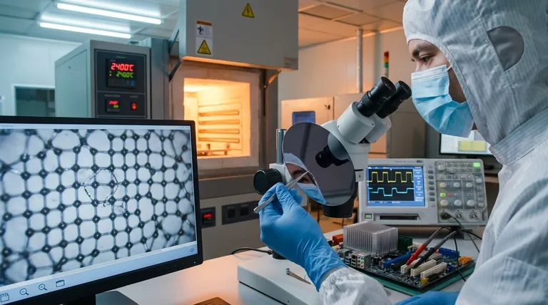
Silicon carbide crystals, or boules, are grown using a process called Physical Vapor Transport (PVT) at extremely high temperatures, often exceeding 2,400°C. This is more than 1,000°C hotter than the process for growing silicon ingots.
This energy-intensive process is slow and difficult to control, limiting the size of wafers that can be produced and directly contributing to their high cost.
The Problem of Defect Density
The harsh growth conditions result in a higher concentration of crystalline imperfections in SiC wafers compared to silicon. These defects, such as micropipes and basal plane dislocations, can act as failure points within a device.
A higher defect density reduces the manufacturing yield, meaning fewer usable chips can be produced from each wafer. This is a primary driver of the higher price for SiC components.
The High Cost of Hardness
Silicon carbide is an exceptionally hard material, ranking just below diamond on the Mohs scale. While this contributes to its ruggedness, it makes slicing wafers from the boule and then grinding and polishing them extremely difficult.
This process consumes more time, requires specialized diamond-coated equipment, and leads to more tool wear, all of which add significant cost to the final wafer.
Device-Level Reliability and Performance Hurdles
Even after a device is manufactured, inherent properties of SiC create specific reliability concerns that must be addressed in the design.
The Unstable Gate Oxide Interface
The interface between the SiC material and the silicon dioxide (SiO₂) gate insulator is the most critical reliability concern in SiC MOSFETs. It is less stable than the near-perfect interface found in silicon MOSFETs.
This instability can cause the device's threshold voltage (Vth) to drift over its lifetime, especially at high temperatures. This drift can impact circuit performance and eventually lead to device failure, demanding careful screening and qualification.
Short-Circuit Fragility
SiC MOSFETs have a much higher power density and smaller chip size than equivalent silicon IGBTs. As a result, they have a very low thermal mass.
During a short-circuit event, their temperature rises incredibly fast, giving them a short-circuit withstand time (SCWT) that is often less than 3 microseconds, compared to 10 microseconds for a typical IGBT. This requires extremely fast and robust protection circuits to prevent catastrophic failure.
Body Diode Limitations
The intrinsic "body diode" within a SiC MOSFET is used for freewheeling current in many applications. However, this diode historically has a higher forward voltage drop compared to silicon equivalents.
This higher voltage drop can lead to increased conduction losses and potential degradation over time. While recent generations of SiC have significantly improved body diode performance, it remains a key parameter to evaluate.
Understanding the Trade-offs: System Integration Complexity
The primary benefit of SiC—its fast switching speed—is also the source of its greatest system-level challenges. Using SiC effectively means designing the entire system around it.
The Double-Edged Sword of Fast Switching
SiC devices can switch on and off orders of magnitude faster than silicon. These high dv/dt (rate of change of voltage) and di/dt (rate of change of current) rates are what reduce switching losses and enable smaller components.
However, these same fast edges interact with parasitic inductance in the circuit layout, causing significant voltage overshoot and ringing. This electrical noise can exceed component voltage ratings, damage the device, and degrade system reliability.
Managing Increased Electromagnetic Interference (EMI)
The high-frequency noise generated by fast-switching SiC is a potent source of EMI. If not properly managed, this noise can interfere with the operation of nearby electronics.
Controlling EMI requires meticulous PCB layout, shielding, and the addition of filtering components, all of which add complexity and cost to the design process.
The Need for Specialized Gate Drivers
Driving a SiC MOSFET is more demanding than driving a silicon IGBT or MOSFET. They often require a negative turn-off voltage (e.g., -5V) to prevent parasitic turn-on caused by the high dv/dt.
The gate driver circuit must be placed very close to the device and be capable of providing high peak currents to switch the device quickly while mitigating the effects of noise and ringing.
Making an Informed Decision on SiC
Successfully implementing silicon carbide requires acknowledging these challenges as engineering problems to be solved, not as insurmountable roadblocks.
- If your primary focus is maximum power density and efficiency: The performance gains are likely worth the effort, but you must invest heavily in advanced PCB layout, robust gate drivers, and managing EMI.
- If your primary focus is cost-sensitivity: Evaluate the total system cost, not just the device cost. SiC may allow you to save money by using smaller inductors, capacitors, and heat sinks, potentially offsetting its higher component price.
- If your primary focus is long-term reliability: Pay extreme attention to the gate driver design, implement ultra-fast short-circuit protection, and select devices from manufacturers with proven data on gate oxide stability.
Understanding these inherent challenges is the first step to unlocking the transformative performance of silicon carbide technology.
Summary Table:
| Challenge Category | Key Issues | Impact on Design |
|---|---|---|
| Manufacturing & Material | High-temperature crystal growth, high defect density, material hardness | Higher component cost, lower yield |
| Device-Level Reliability | Gate oxide instability, short-circuit fragility, body diode limitations | Requires robust protection circuits and careful qualification |
| System Integration | Fast switching causing voltage overshoot, EMI, need for specialized gate drivers | Demands meticulous PCB layout, shielding, and filtering |
Ready to overcome the challenges of silicon carbide in your lab? KINTEK specializes in providing high-quality lab equipment and consumables tailored for advanced material research and development. Whether you're working on SiC crystal growth, device testing, or system integration, our solutions are designed to enhance your efficiency and reliability. Contact us today to learn how we can support your laboratory's specific needs and help you achieve breakthrough results with silicon carbide technology.
Visual Guide
Related Products
- Silicon Carbide (SIC) Ceramic Sheet Wear-Resistant Engineering Advanced Fine Ceramics
- Silicon Carbide (SIC) Ceramic Plate for Engineering Advanced Fine Ceramics
- Silicon Carbide (SIC) Ceramic Sheet Flat Corrugated Heat Sink for Engineering Advanced Fine Ceramics
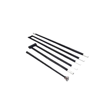
- Silicon Carbide SiC Thermal Heating Elements for Electric Furnace
- Precision Machined Silicon Nitride (SiN) Ceramic Sheet for Engineering Advanced Fine Ceramics
People Also Ask
- What are the applications of silicon carbide? From Abrasives to High-Tech Semiconductors
- What are the uses of silicon carbide ceramics in different industries? Master Extreme Performance in Aerospace, Semiconductors & More
- What is the strongest ceramics? Silicon Carbide Leads in Hardness & Thermal Strength
- What are the properties of SiC? Unlock High-Temperature, High-Frequency Performance
- Why is silicon carbide more efficient? Unlock Higher Power Density with SiC's Superior Material Properties