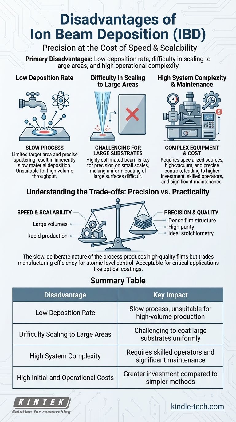
In short, the primary disadvantages of ion beam deposition are its low deposition rate, difficulty in scaling to large surface areas, and high operational complexity. This PVD technique is highly precise, but that precision comes at the cost of speed and scalability, making it unsuitable for applications requiring high-volume throughput or the uniform coating of large substrates.
While ion beam deposition produces exceptionally high-quality thin films with superior density and adhesion, its core drawbacks are rooted in the trade-off between this precision and manufacturing efficiency. The method is fundamentally complex, slow, and difficult to scale.

The Primary Limitations Explained
Ion beam deposition (IBD) is valued for its control, but the very mechanisms that provide this control also create its most significant limitations. Understanding these is critical for selecting the right deposition process.
Low Deposition Rate
The process works by using a highly controlled ion beam to sputter, or eject, atoms from a target material one by one. This meticulous process is inherently slow compared to other deposition methods.
The limited target area that can be effectively sputtered by the ion beam further constrains the overall rate at which material can be deposited onto the substrate.
Difficulty in Scaling to Large Areas
The ion beam used in IBD is highly collimated, meaning the ions travel in a straight, parallel path. This is key to achieving precision and uniform film thickness on a small scale.
However, this same characteristic makes it very challenging to uniformly coat large surfaces. While techniques like dual ion beam sputtering exist, the fundamental limitation of the target area makes IBD a poor choice for large-scale applications.
High System Complexity and Maintenance
IBD systems are sophisticated pieces of equipment. They require specialized ion sources, high-vacuum chambers, and precise control systems to manage the process variables.
This complexity translates directly into higher initial investment costs, the need for skilled operators, and significant ongoing maintenance requirements compared to simpler deposition techniques.
Understanding the Trade-offs: Precision vs. Practicality
The disadvantages of ion beam deposition cannot be viewed in isolation. They are the direct consequence of its greatest strengths, creating a clear set of trade-offs for engineers and researchers.
The Benefit of Unmatched Control
The reason to accept IBD's drawbacks is the unparalleled quality of the resulting film. The process allows for independent and precise control over deposition parameters.
This control imparts valuable properties to the film, including a dense structure, superior adhesion, high purity, fewer defects, and ideal stoichiometry that are difficult to achieve with other methods.
The Inherent Cost of Quality
The slow, deliberate nature of the sputtering process is exactly what produces these high-quality films. You are trading manufacturing speed and volume for atomic-level control.
For applications where film performance is the absolute priority—such as in optical coatings or advanced semiconductor research—this trade-off is often deemed acceptable.
Potential for Unintended Film Modification
The high-energy ions interact directly with the substrate and the growing film, leading to processes like implantation and scattering.
While this can be harnessed to modify film properties advantageously (e.g., increasing density), it also represents a complexity that must be carefully managed. If not properly controlled, these interactions can unintentionally alter the film's crystal structure or composition.
Making the Right Choice for Your Application
Ultimately, the "disadvantages" of ion beam deposition are only disadvantages if they conflict with your primary goal.
- If your primary focus is high-volume production or coating large substrates: The low deposition rate and poor scalability of IBD make it an impractical choice.
- If your primary focus is creating high-purity, dense films with precise stoichiometry for critical components: The disadvantages of IBD are an acceptable price to pay for its superior control and quality.
Choosing the right deposition technique requires aligning the process's capabilities with your project's specific balance of film performance and manufacturing efficiency.
Summary Table:
| Disadvantage | Key Impact |
|---|---|
| Low Deposition Rate | Slow process, unsuitable for high-volume production |
| Difficulty Scaling to Large Areas | Challenging to coat large substrates uniformly |
| High System Complexity | Requires skilled operators and significant maintenance |
| High Initial and Operational Costs | Greater investment compared to simpler methods |
Need a deposition solution tailored to your lab's unique requirements? At KINTEK, we specialize in providing high-quality lab equipment, including advanced deposition systems. Whether you're prioritizing precision for critical research or efficiency for larger-scale projects, our experts can help you select the ideal equipment to meet your goals. Contact us today to optimize your thin-film processes with KINTEK's reliable solutions!
Visual Guide
Related Products
- Chemical Vapor Deposition CVD Equipment System Chamber Slide PECVD Tube Furnace with Liquid Gasifier PECVD Machine
- HFCVD Machine System Equipment for Drawing Die Nano-Diamond Coating
- Electron Beam Evaporation Coating Oxygen-Free Copper Crucible and Evaporation Boat
- RF PECVD System Radio Frequency Plasma-Enhanced Chemical Vapor Deposition RF PECVD
- Customer Made Versatile CVD Tube Furnace Chemical Vapor Deposition Chamber System Equipment
People Also Ask
- What happens during deposition chemistry? Building Thin Films from Gaseous Precursors
- What types of substrates are used in CVD to facilitate graphene films? Optimize Graphene Growth with the Right Catalyst
- What are the processes of vapor phase deposition? Understand CVD vs. PVD for Superior Thin Films
- What are the advantages of chemical vapor deposition? Achieve Superior Thin Films for Your Lab
- What is the chemical vapor deposition growth process? Build Superior Thin Films from the Atom Up


