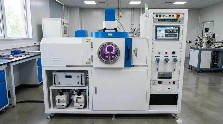
The primary parameters of RF sputtering are the power source frequency, operating pressure, power level, and the type of inert gas used. These factors work together to control the plasma environment and, consequently, the rate and quality of the thin film deposition.
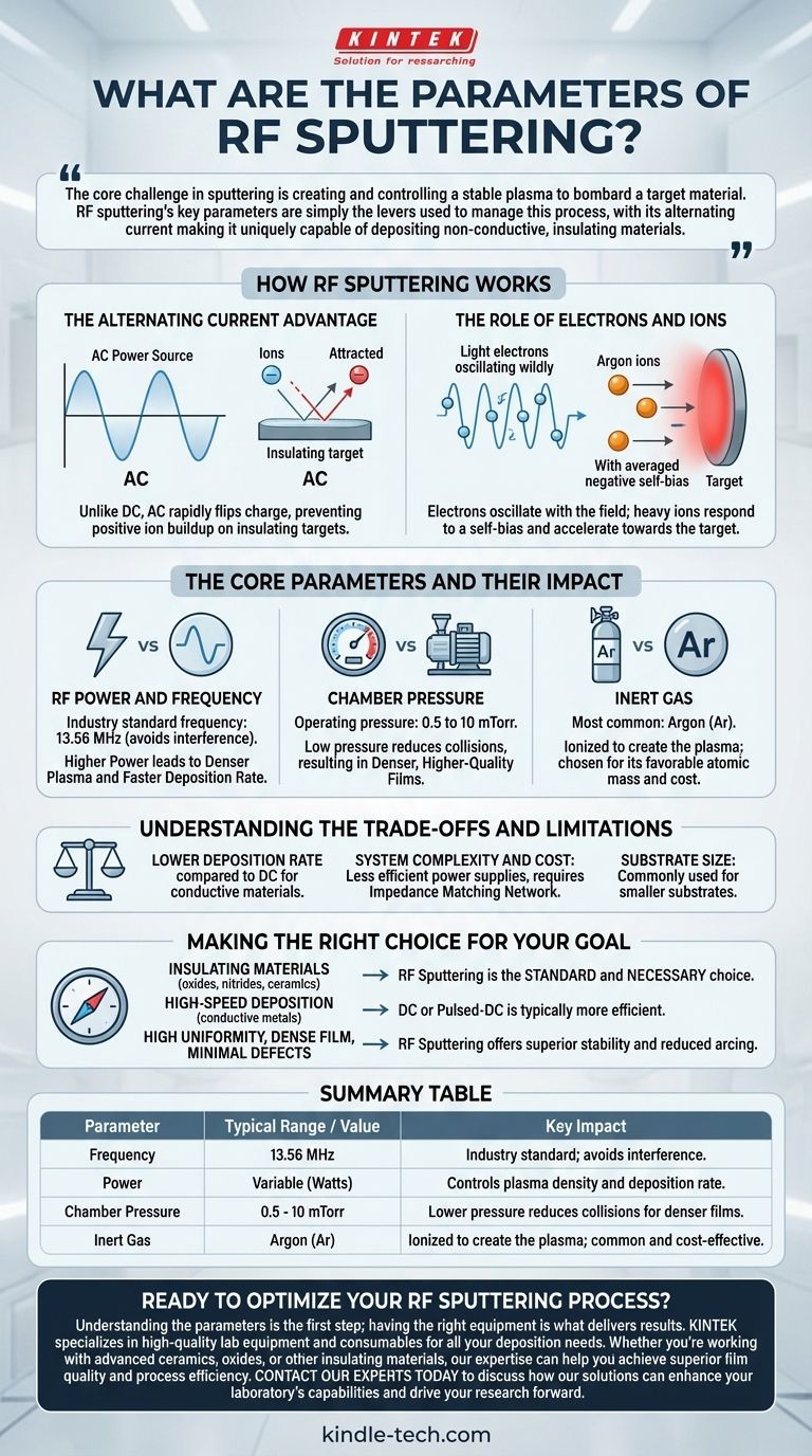
The core challenge in sputtering is creating and controlling a stable plasma to bombard a target material. RF sputtering's key parameters are simply the levers used to manage this process, with its alternating current making it uniquely capable of depositing non-conductive, insulating materials.
How RF Sputtering Works
The Alternating Current Advantage
Unlike DC sputtering, which uses a constant negative voltage, RF sputtering employs an Alternating Current (AC) power source. This rapidly flips the charge on the target material.
This oscillation is the key to sputtering insulating (dielectric) materials. A constant DC voltage would cause positive ion charges to build up on an insulating target, repelling further ions and quickly stopping the sputtering process.
The Role of Electrons and Ions
The AC field affects electrons and ions differently due to their vast difference in mass. The lightweight electrons are able to oscillate with the high-frequency field.
Heavier gas ions (like Argon) cannot keep up with the rapid switching. Instead, they respond to an averaged negative charge, or self-bias, that naturally forms on the target surface, accelerating them toward the target to cause sputtering.
The Core Parameters and Their Impact
RF Power and Frequency
The industry standard frequency is fixed at 13.56 MHz. This specific frequency is chosen to avoid interfering with radio and communication bands.
The RF power level, often measured in watts, directly controls the energy of the plasma. Higher power generally leads to a denser plasma, which increases the sputtering rate and film deposition speed.
Chamber Pressure
RF sputtering operates at a relatively low pressure, typically between 0.5 to 10 mTorr (millitorr).
This low pressure is advantageous because it reduces the chance of sputtered atoms colliding with gas atoms on their way to the substrate. This results in a more direct "line-of-sight" deposition and can lead to higher-quality, denser films.
Inert Gas
An inert gas, most commonly Argon (Ar), is introduced into the vacuum chamber. It is this gas that is ionized to create the plasma.
The choice of gas can affect the sputter yield, but Argon is typically selected for its favorable combination of atomic mass and cost.
Understanding the Trade-offs and Limitations
Lower Deposition Rate
A significant trade-off is that RF sputtering generally has a lower deposition rate compared to DC sputtering for conductive materials.
System Complexity and Cost
The equipment is more complex and expensive. RF power supplies are less efficient than their DC counterparts and require a sophisticated impedance matching network between the power supply and the chamber to deliver power effectively.
Substrate Size
Partly due to the complexity and cost of scaling the equipment, RF sputtering is most commonly used for depositing films on smaller substrates.
Making the Right Choice for Your Goal
- If your primary focus is depositing insulating materials (like oxides, nitrides, or ceramics): RF sputtering is the standard and necessary choice, as DC sputtering is not a viable option.
- If your primary focus is high-speed deposition of conductive metals: DC or Pulsed-DC magnetron sputtering is typically the more efficient and cost-effective solution.
- If your primary focus is achieving a highly uniform, dense film with minimal defects: The stability of the RF plasma at low pressures and its reduction of arcing make it a superior choice.
Understanding these parameters allows you to select the correct deposition technique and tune the process to achieve your desired film properties.
Summary Table:
| Parameter | Typical Range / Value | Key Impact |
|---|---|---|
| Frequency | 13.56 MHz | Industry standard; avoids interference. |
| Power | Variable (Watts) | Controls plasma density and deposition rate. |
| Chamber Pressure | 0.5 - 10 mTorr | Lower pressure reduces collisions for denser films. |
| Inert Gas | Argon (Ar) | Ionized to create the plasma; common and cost-effective. |
Ready to Optimize Your RF Sputtering Process?
Understanding the parameters is the first step; having the right equipment is what delivers results. KINTEK specializes in high-quality lab equipment and consumables for all your deposition needs. Whether you're working with advanced ceramics, oxides, or other insulating materials, our expertise can help you achieve superior film quality and process efficiency.
Contact our experts today to discuss how our solutions can enhance your laboratory's capabilities and drive your research forward.
Visual Guide
Related Products
- RF PECVD System Radio Frequency Plasma-Enhanced Chemical Vapor Deposition RF PECVD
- Horizontal High Temperature Graphite Vacuum Graphitization Furnace
- Spark Plasma Sintering Furnace SPS Furnace
- Automatic Laboratory Hydraulic Press for XRF & KBR Pellet Press
- Electron Beam Evaporation Coating Oxygen-Free Copper Crucible and Evaporation Boat
People Also Ask
- How does Radio Frequency Enhanced Plasma Chemical Vapour Deposition (RF-PECVD) work? Learn the Core Principles
- What is plasma chemical vapor deposition? A Low-Temperature Thin Film Coating Solution
- What is plasma enhanced chemical Vapour deposition process used for fabrication of? A Guide to Low-Temperature Thin Films
- What is an example of PECVD? RF-PECVD for High-Quality Thin Film Deposition
- What is plasma CVD? Unlock Low-Temperature Thin Film Deposition for Sensitive Materials


