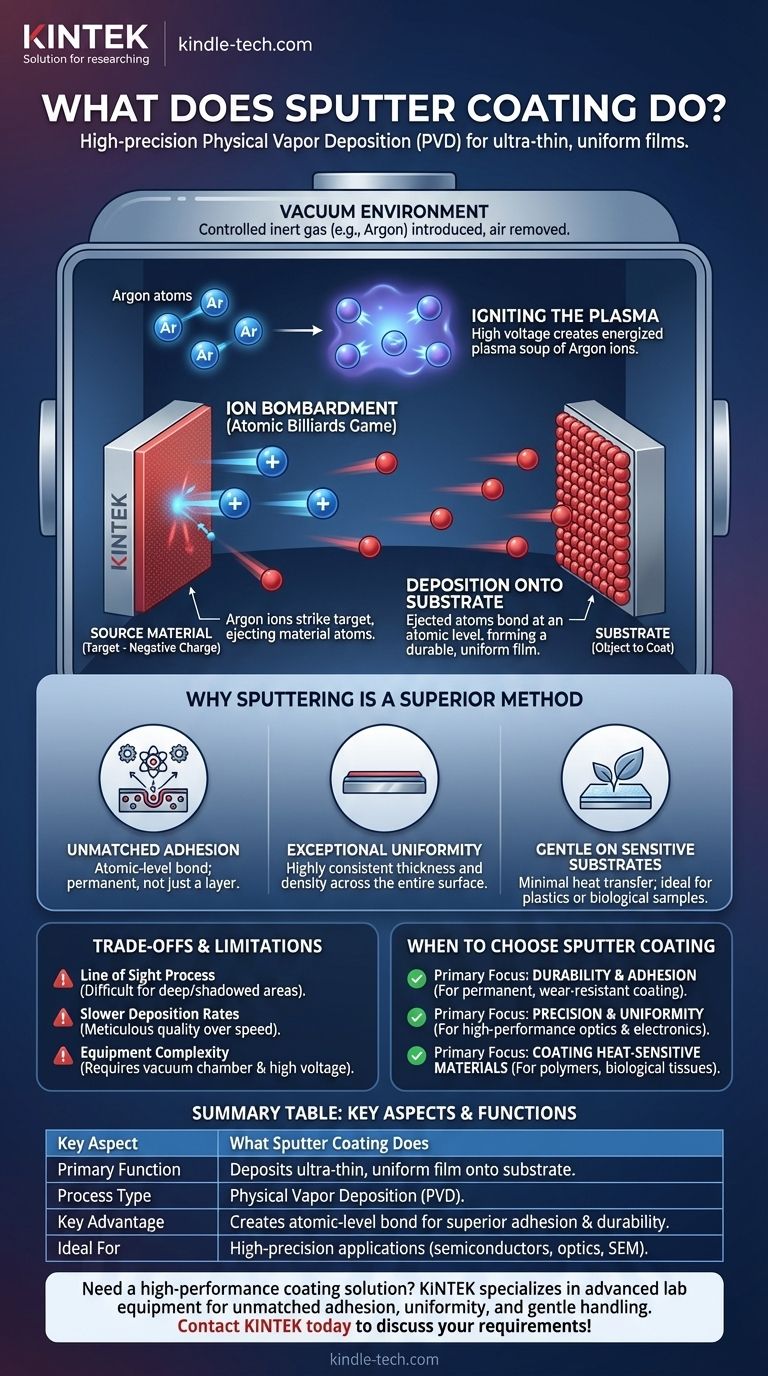
In essence, sputter coating is a high-precision process that deposits an ultra-thin, uniform film of material onto a surface. It works by using energized gas ions in a vacuum to physically knock atoms off a source material (the "target"), which then travel and condense onto the object you wish to coat (the "substrate"). This method creates a bond at the atomic level, making the coating incredibly durable and consistent.
Sputter coating is not merely applying a layer; it's a physical vapor deposition (PVD) technique that embeds atoms into a surface. This creates an exceptionally strong, uniform, and durable atomic-level bond that is fundamentally superior to simple plating or painting for high-performance applications.
The Sputtering Process: An Atomic Billiards Game
To understand what sputter coating does, it helps to visualize it as a controlled game of billiards happening at an atomic scale. The entire process takes place inside a sealed vacuum chamber to ensure purity.
The Vacuum Environment
First, the chamber is evacuated to remove air and other contaminants. It is then backfilled with a small, controlled amount of a high-purity inert gas, most commonly Argon.
Igniting the Plasma
A high voltage is applied, which strips electrons from the Argon atoms. This creates an energized soup of positive Argon ions and free electrons known as a plasma, which often glows purple or blue.
The Ion Bombardment
The source material, or target, is given a negative electrical charge. This attracts the positively charged Argon ions from the plasma, causing them to accelerate and collide with the target at high speed.
This bombardment is a momentum transfer process. Each ion acts like a cue ball, striking the target atoms and ejecting them from the surface with significant force.
Deposition onto the Substrate
These ejected target atoms travel through the vacuum chamber and strike the substrate. Because they arrive with high energy, they embed themselves into the substrate's surface, forming an incredibly strong and dense film.
Why Sputtering is a Superior Coating Method
The unique nature of the sputtering process provides several key advantages that make it essential in fields ranging from semiconductor manufacturing to preparing biological samples for microscopy.
Unmatched Adhesion
Unlike paint, which simply sits on a surface, sputtered atoms are driven into the substrate. This creates a powerful atomic-level bond, making the coating a permanent part of the object rather than just an applied layer.
Exceptional Uniformity
The stable and controlled plasma ensures that atoms are ejected from the target evenly. This results in a film of highly consistent thickness and density across the entire surface of the substrate, which is critical for optical and electronic components.
Gentle on Sensitive Substrates
While the overall process generates some heat that must be managed, the sputtered atoms themselves do not transfer significant thermal energy to the substrate. This makes sputtering ideal for coating heat-sensitive materials like plastics or biological samples for a scanning electron microscope (SEM).
Understanding the Trade-offs and Limitations
No technology is perfect for every scenario. Being an effective advisor means acknowledging the practical constraints of sputtering.
The "Line of Sight" Restriction
Sputtering is a "line of sight" process. Atoms travel in a relatively straight path from the target to the substrate. This makes it difficult to coat the inside of deep holes or complex, shadowed areas without rotating the substrate on specialized fixtures.
Slower Deposition Rates
Precision comes at a cost. Sputtering is often a slower deposition method compared to other techniques like thermal evaporation. The meticulous, controlled nature of the process prioritizes quality over speed.
Equipment Complexity
The requirement for a vacuum chamber, high-voltage power supplies, and process controls makes sputtering equipment more complex and expensive than simpler coating methods like electroplating.
When to Choose Sputter Coating
Your choice of coating technology should always be driven by your end goal. Sputtering is the definitive choice when performance and precision are non-negotiable.
- If your primary focus is durability and adhesion: Sputter coating is ideal because it creates an atomic bond, making the coating a permanent and wear-resistant part of the substrate.
- If your primary focus is precision and uniformity: The controlled plasma process ensures a consistent, ultra-thin film, which is critical for high-performance optics, electronics, and SEM sample preparation.
- If your primary focus is coating heat-sensitive materials: Sputtering is a superior choice as it deposits material with minimal heat transfer, protecting the integrity of delicate substrates like polymers or biological tissue.
By understanding its principles of atomic-level deposition, you can leverage sputter coating to achieve a level of performance and quality that is simply unattainable with conventional methods.
Summary Table:
| Key Aspect | What Sputter Coating Does |
|---|---|
| Primary Function | Deposits an ultra-thin, uniform film of material onto a surface (substrate). |
| Process Type | A Physical Vapor Deposition (PVD) technique. |
| Key Advantage | Creates an atomic-level bond for superior adhesion and durability. |
| Ideal For | High-precision applications in semiconductors, optics, and SEM sample preparation. |
Need a high-performance coating solution for your lab?
Sputter coating is the definitive choice when performance and precision are non-negotiable. KINTEK specializes in providing advanced lab equipment and consumables to meet these critical needs. Our solutions ensure unmatched adhesion, exceptional uniformity, and gentle handling of sensitive substrates.
Let our experts help you achieve superior results for your high-performance applications. Contact KINTEK today to discuss your specific coating requirements!
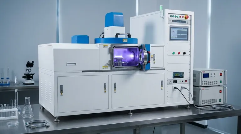
Visual Guide
Related Products
- Infrared Transmission Coating Sapphire Sheet Substrate Window
- Electron Beam Evaporation Coating Oxygen-Free Copper Crucible and Evaporation Boat
- 400-700nm Wavelength Anti Reflective AR Coating Glass
- Custom CVD Diamond Coating for Lab Applications
- Molybdenum Tungsten Tantalum Special Shape Evaporation Boat
People Also Ask
- Why do we need optical coating? To Control Light and Enhance Optical Performance
- What are the applications of optical coating? Unlock Advanced Light Control for Your Industry
- Is Sputter Tint good? Premium Heat Rejection & Long-Term Durability Explained
- What is the optical coating? Master Light Control for Superior Optical Performance
- What is the thinnest coating? Unlocking Unique Properties at the Atomic Scale


