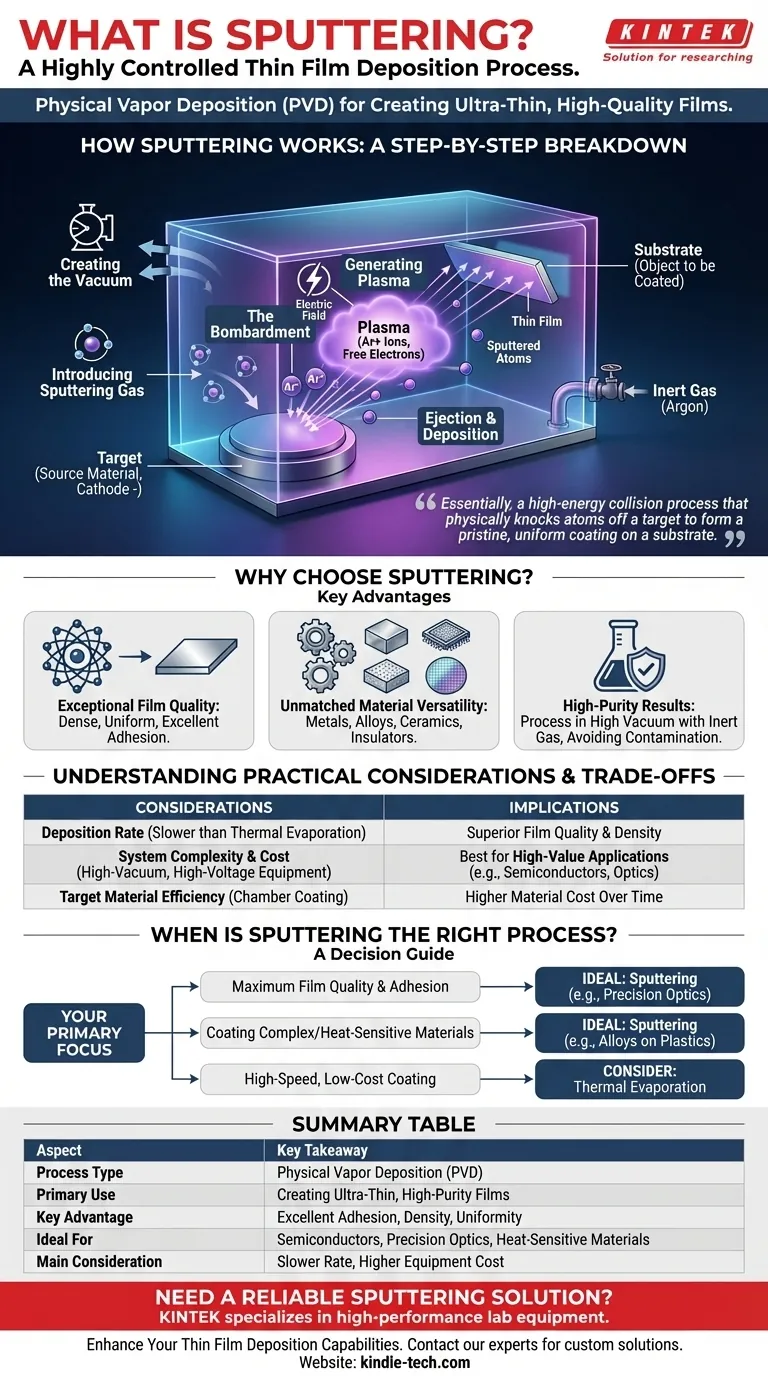
At its core, sputtering is a highly controlled process for creating ultra-thin films on a surface. It works by creating a plasma in a vacuum and using it to bombard a source material, called a target. This high-energy collision physically knocks atoms off the target, which then travel and deposit onto a nearby object, known as the substrate, forming a pristine, uniform coating.
Sputtering is fundamentally a physical vapor deposition (PVD) technique. Its value lies not just in applying a coating, but in its ability to create exceptionally high-quality, dense, and well-adhered thin films from a vast range of materials, making it a cornerstone of modern high-tech manufacturing.
How Sputtering Works: A Step-by-Step Breakdown
The sputtering process happens within a sealed vacuum chamber and relies on a sequence of controlled physical events. Each step is critical to achieving the desired film quality.
The Essential Components
The setup consists of a vacuum chamber containing the material to be coated (substrate) and the source material for the film (target). An inert gas, most commonly Argon, is also required.
Step 1: Creating the Vacuum
First, a deep vacuum is created within the chamber. This removes air and other contaminants that could interfere with the process or become trapped in the thin film, compromising its purity.
Step 2: Introducing the Sputtering Gas
A small, controlled amount of an inert gas like Argon is introduced into the chamber. This gas is not chemically reactive but will serve as the medium for the bombardment.
Step 3: Generating Plasma
A high voltage is applied within the chamber, creating a strong electric field. This field energizes the Argon gas, stripping electrons from the Argon atoms and creating a plasma—an ionized gas consisting of positive Argon ions (Ar+) and free electrons.
Step 4: The Bombardment
The target material is given a negative electrical charge, effectively turning it into a cathode. The positively charged Argon ions in the plasma are aggressively accelerated toward this negatively charged target, colliding with it at high velocity.
Step 5: Ejection and Deposition
The sheer kinetic energy from this ionic bombardment dislodges, or "sputters," individual atoms from the target's surface. These ejected atoms travel in a straight line through the vacuum and strike the substrate, gradually building up a thin film one atomic layer at a time.
Why Choose Sputtering?
While other deposition methods exist, sputtering is chosen for its distinct advantages in precision, quality, and versatility.
Exceptional Film Quality
Sputtering produces films that are incredibly dense, uniform, and have excellent adhesion to the substrate. This is critical in applications like precision optics and semiconductor manufacturing where film performance is paramount.
Unmatched Material Versatility
The process is purely physical, not chemical or thermal. This means it can be used to deposit a huge range of materials, including metals, alloys, ceramics, and other insulating compounds, onto virtually any type of substrate.
High-Purity Results
Because the process occurs in a high vacuum and uses an inert gas, the resulting films are extremely pure. This avoids the contamination that can occur in chemical or heat-based deposition methods.
Understanding the Practical Considerations
While powerful, sputtering is a technical process with specific trade-offs that influence its use.
Deposition Rate
Sputtering is generally a slower process compared to other methods like thermal evaporation. The trade-off is clear: you exchange speed for superior film quality and density.
System Complexity and Cost
The required equipment—including high-vacuum pumps, high-voltage power supplies, and process gas controllers—is complex and expensive. This makes it more suitable for high-value applications than for simple, bulk coating tasks.
Target Material Efficiency
The process is directional, but not perfectly so. Some of the sputtered target material inevitably coats the inside of the chamber walls rather than the substrate, which can impact material usage efficiency over time.
When is Sputtering the Right Process?
Choosing a deposition technique depends entirely on your end goal.
- If your primary focus is maximum film quality and adhesion: Sputtering is the ideal choice for applications like semiconductor layers or precision optical filters where performance cannot be compromised.
- If your primary focus is coating complex or heat-sensitive materials: The low-heat, non-chemical nature of sputtering makes it perfect for depositing alloys, ceramics, or coatings onto delicate substrates like plastics.
- If your primary focus is high-speed, low-cost coating: For applications where film density and purity are less critical, a faster and simpler method like thermal evaporation may be a more economical solution.
Ultimately, sputtering is the definitive choice when you require precise control over the creation of high-performance thin films at the atomic scale.
Summary Table:
| Aspect | Key Takeaway |
|---|---|
| Process Type | Physical Vapor Deposition (PVD) |
| Primary Use | Creating ultra-thin, high-purity films |
| Key Advantage | Excellent film adhesion, density, and uniformity |
| Ideal For | Semiconductors, precision optics, coating heat-sensitive materials |
| Main Consideration | Slower deposition rate, higher equipment cost |
Need a Reliable Sputtering Solution for Your Lab?
KINTEK specializes in high-performance lab equipment, including sputtering systems designed for precision and reliability. Whether you are developing next-generation semiconductors, creating advanced optical coatings, or working with delicate substrates, our expertise ensures you achieve the superior film quality your research demands.
Let us help you enhance your thin film deposition capabilities. Contact our experts today to discuss your specific application and find the perfect sputtering solution for your laboratory needs.
Visual Guide
Related Products
- Spark Plasma Sintering Furnace SPS Furnace
- Lab Sterile Slapping Type Homogenizer for Tissue Mashing and Dispersing
People Also Ask
- What is the process fundamentals of spark plasma sintering? Achieve Rapid, High-Density Material Consolidation
- What is the mechanism of SPS process? A Deep Dive into Rapid, Low-Temperature Sintering
- What are the fundamentals of spark plasma sintering process? Unlock Rapid, High-Performance Material Consolidation
- What is SPS sintering method? A Guide to High-Speed, High-Performance Material Fabrication
- What is the difference between spark plasma sintering and flash sintering? A Guide to Advanced Sintering Methods

