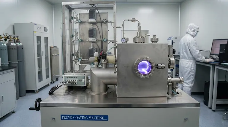
At its core, High-Density Plasma Chemical Vapor Deposition (HDP-CVD) is an advanced thin-film deposition process used primarily in semiconductor manufacturing. Unlike conventional methods, it utilizes a very dense, high-energy plasma to both deposit material and simultaneously sputter (or etch) it away. This unique dual-action mechanism allows it to create extremely high-quality, dense films that can fill very narrow, deep trenches in microchips without creating voids.
The defining characteristic of HDP-CVD is not just its use of plasma, but its ability to perform simultaneous deposition and sputtering. This makes it the industry standard for gap-fill applications where void-free, uniform material is critical.
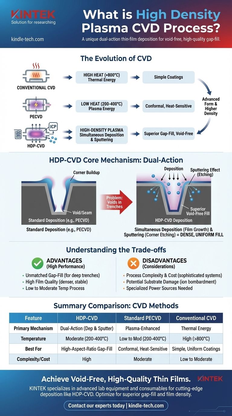
From Conventional CVD to High-Density Plasma
To understand HDP-CVD, it's helpful to see it as an evolution of simpler deposition techniques. Each step in its development was driven by the need to solve a specific engineering problem.
The Foundation: Conventional CVD
The traditional Chemical Vapor Deposition (CVD) process involves introducing precursor gases into a reaction chamber.
High heat provides the energy needed for these gases to react and deposit a solid thin film onto a substrate, such as a silicon wafer. This method is effective for creating uniform coatings on many surfaces.
The Problem with Heat
Conventional CVD operates at very high temperatures, often exceeding 800°C. This extreme heat can damage sensitive components already fabricated on a device and limit the types of materials that can be used as substrates.
The First Evolution: Plasma-Enhanced CVD (PECVD)
Plasma-Enhanced CVD (PECVD) was developed to solve the heat problem. Instead of relying solely on thermal energy, PECVD uses an electric field to create a plasma.
This plasma contains high-energy electrons that provide the necessary energy to drive the chemical reactions at much lower temperatures (typically 200-400°C). This opened the door to coating heat-sensitive materials.
What Makes "High-Density Plasma" Different?
HDP-CVD is a specialized, more advanced form of PECVD. The "high-density" descriptor is the key to its unique capabilities and is defined by two primary factors.
Defining Plasma Density
Plasma density refers to the concentration of ions within the plasma. An HDP reactor generates a plasma with an ion density that is 100 to 10,000 times greater than that of a standard PECVD system.
This is typically achieved using a secondary power source, such as an Inductively Coupled Plasma (ICP) coil, which more efficiently energizes the gas.
The Dual-Action Mechanism: Deposition and Sputtering
This extremely high ion density is what enables the process's signature feature. While the chemical precursors are depositing a film, the high concentration of energetic ions bombarding the wafer surface simultaneously sputters, or etches, material away.
The key is that this sputtering effect is directional and most aggressive on sharp corners and edges.
The Result: Superior Gap-Fill
Imagine filling a narrow trench. In a standard deposition process, material builds up faster on the top corners, potentially sealing the trench before it is completely filled and leaving a void or seam inside.
With HDP-CVD, the sputtering action continuously etches away this corner buildup. This allows the deposition process to proceed all the way to the bottom, resulting in a dense, void-free fill of even very high-aspect-ratio (deep and narrow) structures.
Understanding the Trade-offs
While powerful, HDP-CVD is not the solution for every application. Its benefits come with specific costs and complexities that must be considered.
Advantage: Unmatched Gap-Fill
The primary reason to use HDP-CVD is for its ability to produce void-free films inside deep trenches and complex topographies. This is critical for creating reliable interconnects and insulation layers in modern integrated circuits.
Advantage: High Film Quality
The constant ion bombardment during deposition leads to a denser, more stable, and higher-quality film compared to what is typically achieved with standard PECVD.
Disadvantage: Process Complexity and Cost
HDP-CVD reactors are significantly more complex and expensive than conventional CVD or PECVD systems. They require sophisticated power sources and control systems to manage the balance between deposition and sputtering.
Disadvantage: Potential for Substrate Damage
The same high-energy ion bombardment that enables superior gap-fill can also cause physical damage to the underlying device layers if the process is not meticulously controlled.
Making the Right Choice for Your Goal
Selecting the correct deposition method depends entirely on the geometric constraints and performance requirements of your specific application.
- If your primary focus is depositing a simple, conformal film on a flat or gently sloped surface: Standard PECVD or even thermal CVD is often more cost-effective and perfectly sufficient.
- If your primary focus is filling deep, narrow trenches or vias without creating voids (high-aspect-ratio gap-fill): HDP-CVD is the superior and often necessary choice, essential for advanced device fabrication.
- If your primary focus is coating thermally sensitive devices or substrates: Any plasma-based method like PECVD or HDP-CVD is vastly preferable to high-temperature conventional CVD.
Ultimately, choosing the right deposition technique requires aligning the unique capabilities of the process with the specific material and structural demands of your project.
Summary Table:
| Feature | HDP-CVD | Standard PECVD | Conventional CVD |
|---|---|---|---|
| Primary Mechanism | Simultaneous deposition & sputtering | Plasma-enhanced deposition | Thermal energy deposition |
| Temperature | Moderate (200-400°C) | Low to Moderate (200-400°C) | High (>800°C) |
| Best For | High-aspect-ratio gap-fill, void-free films | Conformal coatings on heat-sensitive materials | Simple, uniform coatings on robust substrates |
| Key Advantage | Superior gap-fill capability | Lower temperature process | Simplicity and wide material compatibility |
| Complexity/Cost | High | Moderate | Low to Moderate |
Ready to achieve void-free, high-quality thin films for your most demanding semiconductor applications?
KINTEK specializes in advanced lab equipment and consumables, providing the precise tools needed for cutting-edge deposition processes like HDP-CVD. Our expertise helps laboratories optimize their semiconductor manufacturing for superior gap-fill and film density.
Contact our experts today to discuss how our solutions can enhance your thin-film deposition capabilities and drive your research forward.
Visual Guide
Related Products
- HFCVD Machine System Equipment for Drawing Die Nano-Diamond Coating
- Microwave Plasma Chemical Vapor Deposition MPCVD Machine System Reactor for Lab and Diamond Growth
- 915MHz MPCVD Diamond Machine Microwave Plasma Chemical Vapor Deposition System Reactor
- Inclined Rotary Plasma Enhanced Chemical Vapor Deposition PECVD Equipment Tube Furnace Machine
- Chemical Vapor Deposition CVD Equipment System Chamber Slide PECVD Tube Furnace with Liquid Gasifier PECVD Machine
People Also Ask
- How expensive is chemical vapor deposition? Understanding the True Cost of High-Performance Coating
- What are the advantages of chemical vapor deposition? Achieve Superior Thin Films for Your Lab
- What is the chemical vapor deposition growth process? Build Superior Thin Films from the Atom Up
- What is the specific function of the metal filament in HF-CVD? Key Roles in Diamond Growth
- What is the hot filament chemical vapour deposition of diamond? A Guide to Synthetic Diamond Coating


