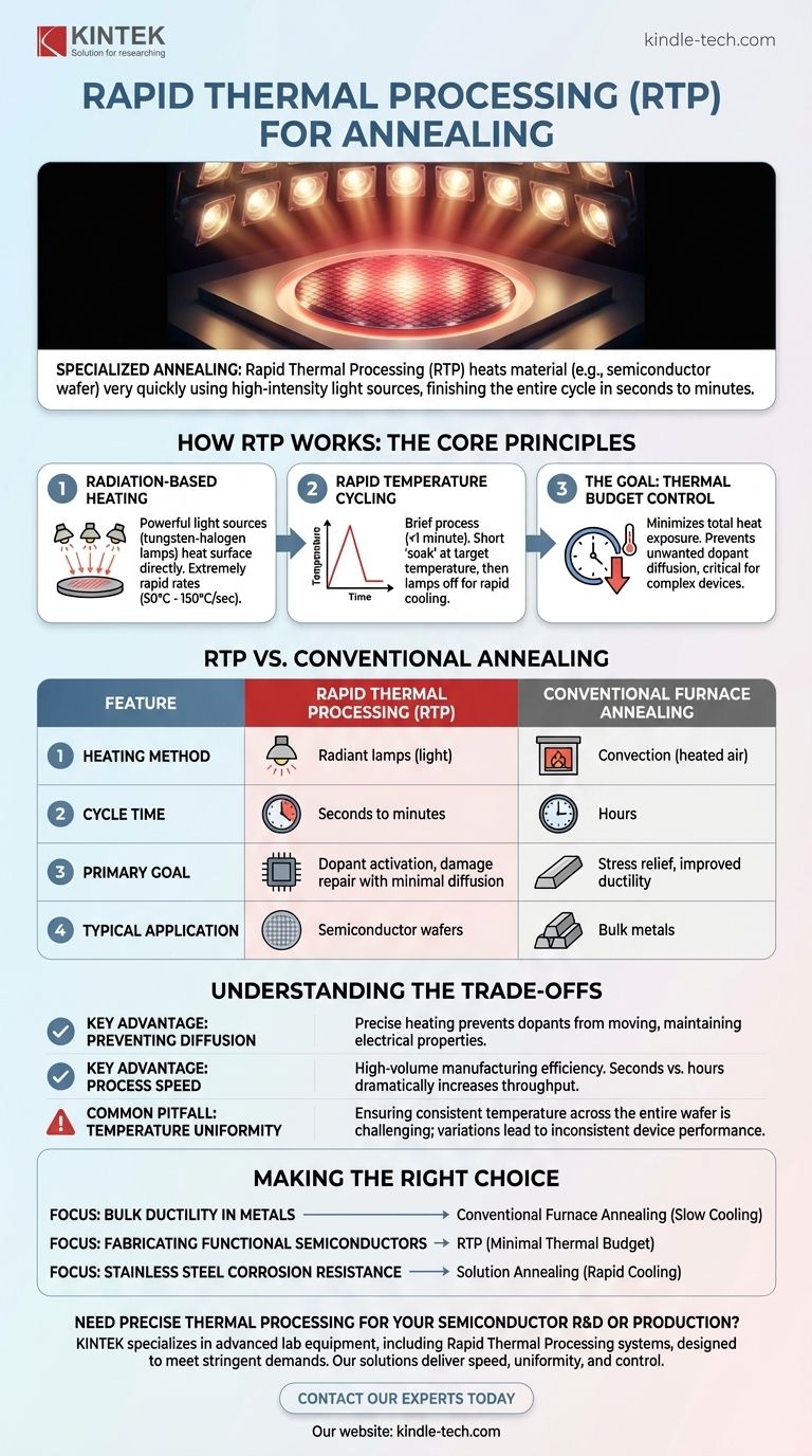
In materials science, Rapid Thermal Processing (RTP) is a specialized annealing method where a material, typically a semiconductor wafer, is heated to high temperatures very quickly using high-intensity light sources. The entire cycle of heating, holding at temperature, and cooling is completed in seconds to minutes, achieving specific structural changes while minimizing unwanted side effects from prolonged heat exposure.
The core purpose of RTP is not just to anneal a material, but to do so with extreme speed and control. This minimizes the total "thermal budget"—the combination of temperature and time—which is critical for fabricating complex, multi-layered devices like modern microchips.
How RTP Works: The Core Principles
While traditional annealing modifies the bulk properties of a material over a long period, RTP is a technique of precision and speed. It achieves the goals of annealing—such as repairing crystal damage or activating dopants—without the drawbacks of a slow furnace.
Radiation-Based Heating
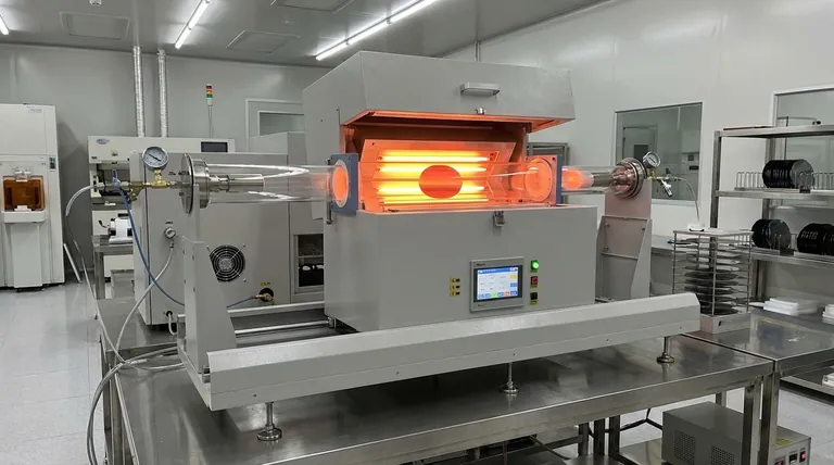
Unlike a conventional furnace that heats materials slowly through convection, RTP uses powerful, incoherent light sources, such as tungsten-halogen lamps. This radiant energy is absorbed directly by the material's surface, enabling extremely rapid heating rates, often between 50°C and 150°C per second.
Rapid Temperature Cycling
The entire RTP process is brief, generally lasting less than a minute. After the short "soak" at the target temperature, the lamps are turned off, and the material cools rapidly. This is a defining feature that separates it from traditional annealing, which emphasizes slow cooling to maximize ductility.
The Goal: Thermal Budget Control
The primary driver for using RTP is to limit the material's total exposure to heat. In complex devices like semiconductors, prolonged heating causes dopant atoms to diffuse or spread out from their intended locations, which can destroy the device's electrical properties. RTP's speed performs the necessary atomic-level repairs without allowing time for this destructive diffusion to occur.
RTP vs. Conventional Annealing
Understanding the context of RTP requires comparing it to traditional methods. The choice between them depends entirely on the material and the desired outcome.
Heating and Cooling Profile
Traditional annealing uses a furnace to slowly heat a material, holds it at temperature, and then cools it very slowly to achieve a relaxed, highly ductile state. RTP does the opposite, employing rapid heating and cooling to achieve a specific, time-sensitive change.
Primary Purpose
Conventional annealing is often used on bulk metals to relieve internal stresses, reverse the effects of work hardening, and improve machinability. Its goal is to make a large piece of material more uniform and workable.
RTP, by contrast, is a key process in semiconductor manufacturing. It is used to activate implanted dopants, repair crystal lattice damage from ion implantation, and form thin films of metal silicides on a wafer.
Material Application
While techniques like solution annealing are used in metallurgy for specific alloys like stainless steel, RTP is almost exclusively associated with the fabrication of integrated circuits on silicon wafers.
Understanding the Trade-offs
RTP is a powerful tool, but its advantages are specific to certain applications, and it comes with unique challenges.
Key Advantage: Preventing Diffusion
As mentioned, the primary benefit of RTP is its ability to heat a wafer just long enough to activate dopants or repair damage without allowing them to move from their precise locations. This precision is impossible to achieve in a conventional furnace.
Key Advantage: Process Speed
In high-volume manufacturing, process time is critical. An RTP cycle that takes 90 seconds is far more efficient than a furnace process that can take many hours, dramatically increasing production throughput.
Common Pitfall: Temperature Uniformity
A significant challenge in RTP is ensuring the entire wafer is heated to the exact same temperature. Any slight variation in lamp intensity or reflectivity across the wafer can create hot or cold spots, leading to inconsistent device performance and lower yields.
Making the Right Choice for Your Goal
Selecting an annealing process is a function of your material, your scale, and your desired structural outcome.
- If your primary focus is improving bulk ductility in metals: Traditional furnace annealing with a slow cooling cycle is the correct approach.
- If your primary focus is fabricating functional semiconductor devices: RTP is essential for activating dopants and repairing damage with minimal thermal budget.
- If your primary focus is enhancing corrosion resistance in stainless steel: A specialized process like solution annealing, which also uses rapid cooling for a different reason, is required.
Ultimately, selecting the correct annealing technique requires matching the process's unique thermal profile to the specific material and desired outcome.
Summary Table:
| Feature | Rapid Thermal Processing (RTP) | Conventional Furnace Annealing |
|---|---|---|
| Heating Method | Radiant lamps (light) | Convection (heated air) |
| Cycle Time | Seconds to minutes | Hours |
| Primary Goal | Dopant activation, damage repair with minimal diffusion | Stress relief, improved ductility |
| Typical Application | Semiconductor wafers | Bulk metals |
Need precise thermal processing for your semiconductor R&D or production?
KINTEK specializes in advanced lab equipment, including Rapid Thermal Processing systems, designed to meet the stringent demands of modern semiconductor fabrication. Our solutions deliver the speed, temperature uniformity, and control you need to maximize yield and performance.
Contact our experts today to discuss how our RTP technology can optimize your annealing process and enhance your device performance.
Visual Guide
Related Products
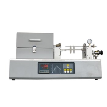
- Laboratory Rapid Thermal Processing (RTP) Quartz Tube Furnace
- Graphite Vacuum Furnace High Thermal Conductivity Film Graphitization Furnace
- Graphite Vacuum Furnace IGBT Experimental Graphitization Furnace
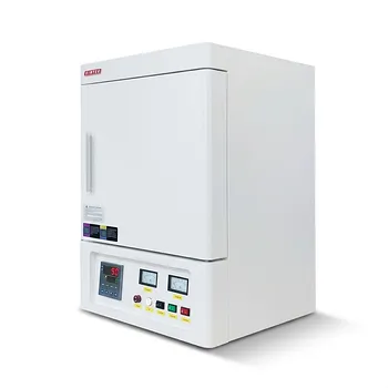
- 1700℃ Muffle Oven Furnace for Laboratory
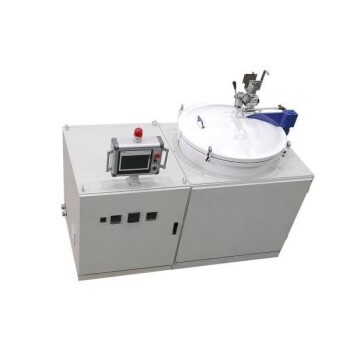
- Small Vacuum Heat Treat and Tungsten Wire Sintering Furnace
People Also Ask
- What is the technical value of using a quartz tube reaction chamber for static corrosion testing? Achieve Precision.
- What happens when quartz is heated? A Guide to Its Critical Phase Transitions and Uses
- What is the function of quartz tubes and vacuum sealing systems? Secure Your High-Purity Solid Solution Synthesis
- What role does a quartz tube furnace play in hBN synthesis? Optimize Your Chemical Vapor Deposition Results
- How do you clean a quartz tube furnace? Prevent Contamination & Extend Tube Lifespan
