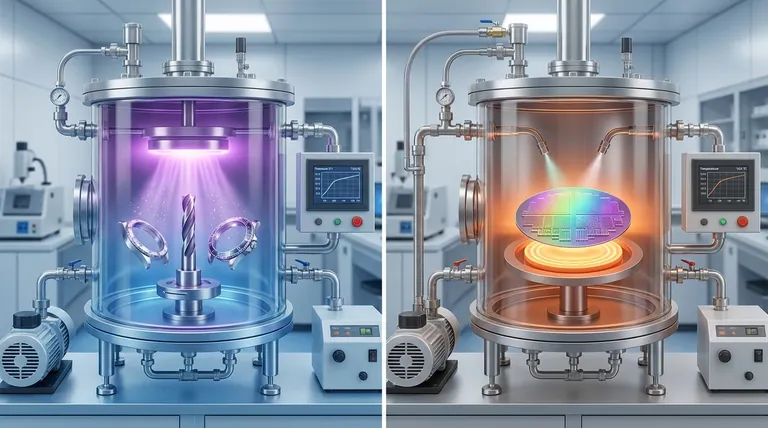
At their core, Physical Vapor Deposition (PVD) and Chemical Vapor Deposition (CVD) are advanced manufacturing processes used to apply extremely thin, functional coatings onto a substrate. These techniques are critical in industries ranging from semiconductors and automotive to architecture and jewelry, where they are used to enhance a material's durability, introduce new electronic properties, or improve its aesthetic appeal.
The choice between PVD and CVD is not about which is "better," but which process is appropriate for the desired outcome. PVD is a physical process ideal for adding hard or decorative coatings at lower temperatures, while CVD is a chemical process essential for creating the highly pure, uniform layers required in applications like microelectronics.
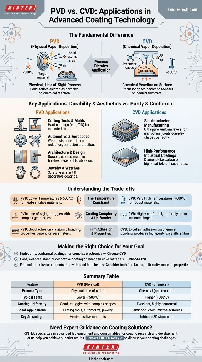
The Fundamental Difference: Process Dictates Application
To understand where each technology is applied, you must first understand how they work. The core distinction lies in how the coating material is transferred to the part's surface.
PVD: A Physical, Line-of-Sight Process
PVD is a physical process, much like spray painting on a microscopic level. In a high vacuum, a solid source material (e.g., titanium) is bombarded with energy, causing atoms or molecules to be ejected.
These ejected particles travel in a straight line and condense onto the substrate, forming a thin, dense film. No fundamental chemical reaction occurs on the substrate's surface.
CVD: A Chemical Reaction on the Surface
CVD is a chemical process. It involves introducing one or more volatile precursor gases into a reaction chamber containing the heated substrate.
These gases decompose and react on the hot surface, forming a new solid material as a coating. This is analogous to how dew forms on a cold surface, but the deposit is the result of a deliberate chemical transformation.
Key Application Areas and Examples
The differences in process directly lead to distinct areas of application where one method has a clear advantage over the other.
PVD Applications: Durability and Aesthetics
Because it is a lower-temperature process, PVD is exceptionally versatile. It is the go-to choice for adding hard, wear-resistant, or decorative coatings to a wide range of materials.
Common applications include:
- Cutting Tools and Molds: Applying coatings like Titanium Nitride (TiN) to improve hardness and extend tool life.
- Automotive and Aerospace: Coating components for wear resistance, friction reduction, and corrosion protection.
- Architecture and Design: Creating durable, colored metallic finishes on fixtures and panels that are resistant to abrasion and fingerprints.
- Jewelry and Watches: Providing scratch-resistant and decorative coatings.
CVD Applications: Purity and Conformal Coatings
CVD excels where film purity and the ability to coat complex shapes are paramount. Its primary domain is the semiconductor industry.
The most critical application is:
- Semiconductor Manufacturing: Creating the ultra-pure, uniform layers of silicon, silicon dioxide, and other materials that form the foundation of microchips and transistors. The gaseous nature of CVD allows it to perfectly coat the microscopic, three-dimensional structures on a silicon wafer.
CVD is also used for high-performance industrial coatings, such as diamond-like carbon, on substrates that can tolerate the high process temperatures.
Understanding the Trade-offs
Choosing between PVD and CVD requires weighing a clear set of engineering trade-offs driven by their underlying processes.
The Temperature Constraint
CVD typically requires very high temperatures (often >600°C) for the chemical reactions to occur. This limits its use to substrates that can withstand extreme heat, such as silicon, ceramics, or refractory metals.
PVD operates at much lower temperatures (often <500°C, sometimes near room temperature). This makes it suitable for coating heat-sensitive materials like alloy steels, aluminum, and even some plastics.
Coating Complexity and Uniformity
Because it relies on gases that fill the entire chamber, CVD provides highly conformal coatings. This means it can uniformly coat intricate shapes and internal surfaces with exceptional precision, which is essential for microelectronics.
As a line-of-sight process, PVD can struggle with complex geometries. Areas that are "shadowed" from the source material may receive a thinner coating or no coating at all, requiring complex part rotation during the process to ensure coverage.
Film Adhesion and Properties
CVD films often exhibit excellent adhesion because the coating is chemically bonded to the substrate. The process can also produce highly pure, dense, crystalline films.
PVD adhesion is generally very good but is based on atomic bonding rather than a chemical reaction. The properties of PVD films are highly dependent on the specific deposition parameters used.
Making the Right Choice for Your Goal
Your application's specific requirements for temperature, geometry, and film properties will guide your decision.
- If your primary focus is high-purity, conformal coatings for complex electronics: CVD is the established standard for its ability to create uniform, high-quality films on intricate structures.
- If your primary focus is applying a hard, wear-resistant, or decorative coating on heat-sensitive materials: PVD is the superior choice because its lower operating temperatures prevent damage to the substrate.
- If your primary focus is enhancing the surface of a tool or component that can withstand high heat: Both technologies are options, but the decision will depend on the desired film thickness, uniformity, and specific material properties.
Ultimately, understanding the core process—physical deposition versus chemical reaction—is the key to selecting the technology that best aligns with your material, geometry, and performance requirements.
Summary Table:
| Feature | PVD (Physical Vapor Deposition) | CVD (Chemical Vapor Deposition) |
|---|---|---|
| Process Type | Physical (line-of-sight) | Chemical (gas reaction) |
| Typical Temperature | Lower (<500°C) | Higher (>600°C) |
| Coating Uniformity | Good, but can struggle with complex shapes | Excellent, highly conformal |
| Ideal Applications | Cutting tools, automotive parts, jewelry, decorative coatings | Semiconductors, microelectronics, high-purity industrial coatings |
| Key Advantage | Works on heat-sensitive materials | Superior for intricate 3D structures |
Need Expert Guidance on Coating Solutions?
Choosing between PVD and CVD is critical for your project's success. The right coating technology can enhance durability, improve performance, and extend the life of your components.
KINTEK specializes in advanced lab equipment and consumables for coating research and development. Whether you are developing new semiconductor materials, enhancing tool durability, or creating innovative decorative finishes, we provide the reliable equipment and expert support you need.
Let us help you achieve superior results. Our team understands the nuances of both PVD and CVD processes and can guide you to the optimal solution for your specific application and material requirements.
Contact KINTEK today to discuss your coating challenges and discover how our solutions can drive your innovation forward.
Visual Guide
Related Products
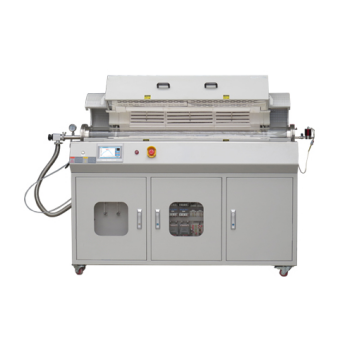
- Chemical Vapor Deposition CVD Equipment System Chamber Slide PECVD Tube Furnace with Liquid Gasifier PECVD Machine
- Inclined Rotary Plasma Enhanced Chemical Vapor Deposition PECVD Equipment Tube Furnace Machine
- RF PECVD System Radio Frequency Plasma-Enhanced Chemical Vapor Deposition RF PECVD
- Customer Made Versatile CVD Tube Furnace Chemical Vapor Deposition Chamber System Equipment
- Vacuum Hot Press Furnace Machine for Lamination and Heating
People Also Ask
- How is PECVD different from CVD? Unlock Low-Temperature Thin Film Deposition
- What is the precursor gas in PECVD? The Key to Low-Temperature Thin Film Deposition
- What are the examples of CVD method? Discover the Versatile Applications of Chemical Vapor Deposition
- What is the difference between thermal CVD and PECVD? Choose the Right Thin-Film Deposition Method
- How are PECVD and CVD different? A Guide to Choosing the Right Thin-Film Deposition Process