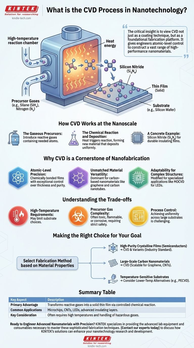
In nanotechnology, Chemical Vapor Deposition (CVD) is a process for building materials atom-by-atom. It works by introducing reactive gases into a chamber, where they undergo a chemical reaction and deposit a new, solid thin film onto a target surface, known as a substrate. This method is fundamental to nanotechnology because it offers the precision needed to create high-quality, ultra-thin materials like graphene and the complex layers used in modern microchips.
The critical insight is to view CVD not just as a coating technique, but as a foundational fabrication platform. It gives engineers atomic-level control to construct a vast range of high-performance nanomaterials that would be impossible to create otherwise.
How CVD Works at the Nanoscale
At its core, the CVD process is a controlled chemical reaction that transforms gases into a solid. This transformation is what allows for the precise construction of nanomaterials.
The Gaseous Precursors
The process begins by introducing two or more gases, called precursors, into a high-temperature reaction chamber. These gases are specifically chosen because they contain the atoms needed for the final material.
The Chemical Reaction and Deposition
Inside the chamber, the heat provides the energy needed to trigger a chemical reaction between the precursor gases. This reaction forms a new, solid material that then deposits uniformly onto a substrate, such as a silicon wafer, building the desired film one atomic layer at a time.
A Concrete Example: Silicon Nitride
A common example is the creation of silicon nitride (Si₃N₄), a durable insulating material. Gaseous silane (SiH₄) and nitrogen (N₂) are introduced into the chamber. They react to form solid silicon nitride, which deposits onto the wafer, creating a chemically bonded, high-purity film.
Why CVD is a Cornerstone of Nanofabrication
CVD isn't just one option among many; it is often the most effective method for synthesizing high-quality nanomaterials due to its unique combination of precision, versatility, and speed.
Atomic-Level Precision
CVD enables the creation of chemically bonded thin films with exceptional control over thickness and purity. This precision is essential for fabricating the high-performance structures required in nanoelectronics and power electronics.
Unmatched Material Versatility
The process is incredibly versatile and is used to create a wide array of nanomaterials. It is the dominant method for producing carbon-based nanomaterials, including graphene, carbon nanotubes (CNTs), and fullerenes.
Adaptability for Complex Structures
The core CVD technique can be modified for highly specialized applications. For instance, Metal-Organic Chemical Vapor Deposition (MOCVD) is a variant used to grow intricate, single-crystal layers on semiconducting wafers, which is a critical step in manufacturing LEDs and high-frequency transistors.
Understanding the Trade-offs
While powerful, the CVD process is not without its challenges. Understanding its limitations is key to its successful application.
High-Temperature Requirements
Many CVD processes require very high temperatures to initiate the chemical reactions. This can limit the types of substrate materials that can be used, as some may be damaged or melt under such conditions.
Precursor Gas Complexity
The precursor gases used in CVD can be highly toxic, flammable, or corrosive. This necessitates sophisticated safety protocols and handling equipment, adding to the overall cost and complexity of the operation.
Process Control
Achieving a perfectly uniform film across a large substrate is challenging. It requires precise control over multiple variables simultaneously, including temperature, pressure, and gas flow rates, making process optimization a complex task.
Making the Right Choice for Your Goal
Selecting the right fabrication method depends entirely on the properties of the material you need to create.
- If your primary focus is high-purity crystalline films for semiconductors: CVD and its variants are the industry standard due to their unparalleled quality and control.
- If your primary focus is large-scale production of carbon nanomaterials: CVD is one of the most scalable and effective methods for producing high-quality graphene and carbon nanotubes.
- If your primary focus is coating a temperature-sensitive substrate: Traditional high-temperature CVD is likely unsuitable, and you should investigate lower-temperature alternatives like Plasma-Enhanced CVD (PECVD).
Ultimately, understanding the principles of CVD is the first step toward engineering the next generation of advanced materials.
Summary Table:
| Key Aspect | Description |
|---|---|
| Core Principle | Transforms reactive gases into a solid thin film on a substrate via a controlled chemical reaction. |
| Primary Advantage | Offers atomic-level precision for creating high-purity, uniform materials like graphene and silicon nitride. |
| Common Applications | Fabrication of microchips, carbon nanotubes (CNTs), LEDs, and advanced insulating layers. |
| Key Consideration | Often requires high temperatures and careful handling of specialized, sometimes hazardous, precursor gases. |
Ready to Engineer Advanced Nanomaterials with Precision?
The CVD process is the foundation for creating the high-performance materials that power modern technology. KINTEK specializes in providing the advanced lab equipment and consumables necessary to master these sophisticated fabrication techniques.
Whether you are developing next-generation semiconductors, synthesizing graphene, or growing complex crystalline structures, our expertise supports your innovation from R&D to production.
Contact our experts today to discuss how KINTEK's solutions can enhance your nanotechnology research and development.
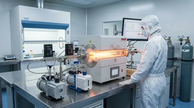
Visual Guide
Related Products
- CVD Diamond Dressing Tools for Precision Applications
- Multi Heating Zones CVD Tube Furnace Machine Chemical Vapor Deposition Chamber System Equipment
- CVD Diamond Domes for Industrial and Scientific Applications
- CVD Diamond for Thermal Management Applications
- Chemical Vapor Deposition CVD Equipment System Chamber Slide PECVD Tube Furnace with Liquid Gasifier PECVD Machine
People Also Ask
- What is CVD diamond? The Ultimate Guide to Lab-Grown Diamonds and Their Uses
- Does the chemical vapor deposition be used for diamonds? Yes, for Growing High-Purity Lab Diamonds
- How do CVD diamonds grow? A Step-by-Step Guide to Lab-Grown Diamond Creation
- How long does it take to make synthetic diamonds? Discover the 6-8 Week Science Behind Lab-Grown Gems
- What are the raw materials for CVD diamonds? A seed, a gas, and the science of crystal growth.


