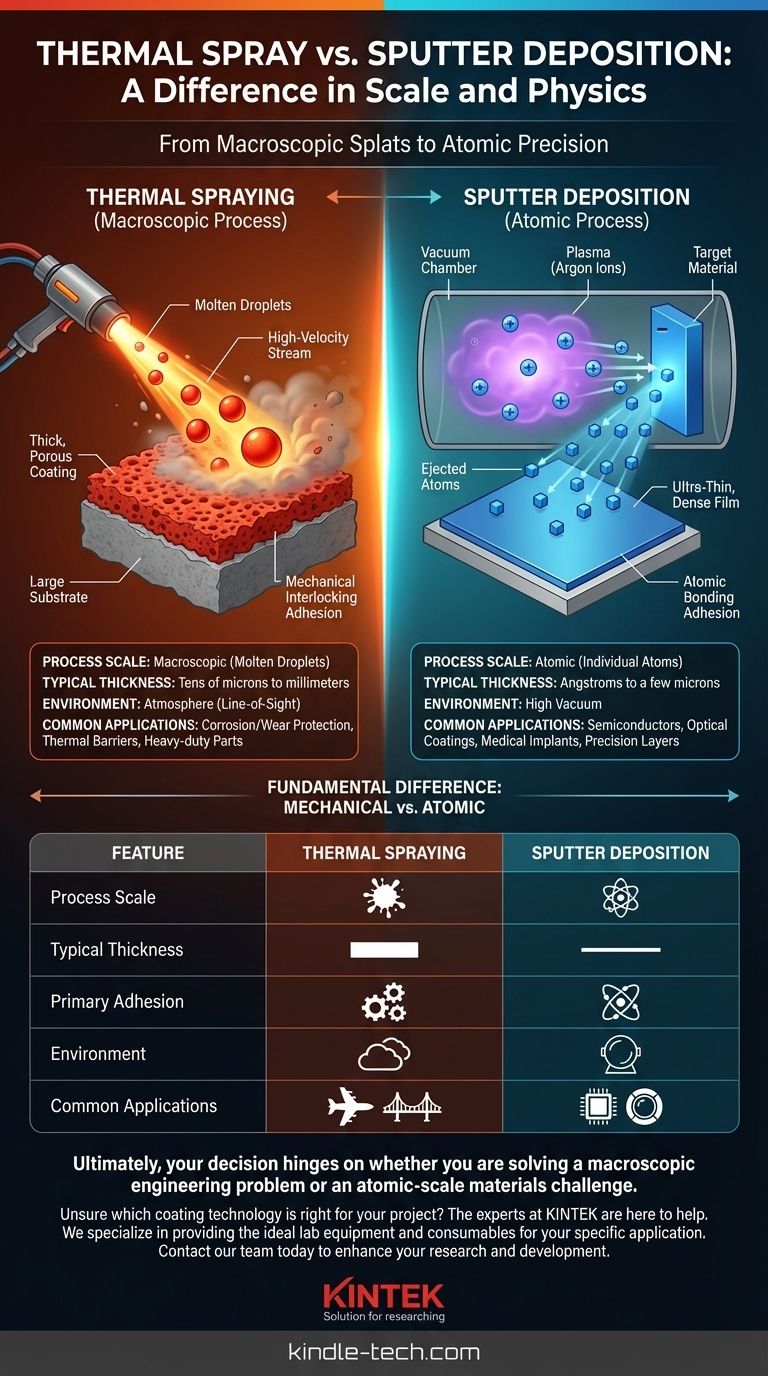
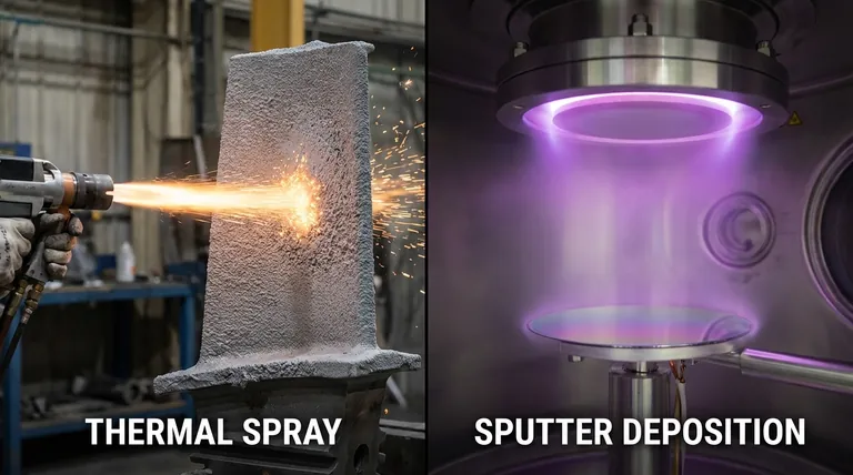
At a fundamental level, the difference between spray and sputter deposition is one of scale and physics. Thermal spraying is a mechanical process that propels molten or semi-molten droplets to form a thick coating, much like a high-tech spray paint. Sputtering is a vacuum-based, atomic-scale process where individual atoms are ejected from a source material by ion bombardment to build an ultra-thin film, one atom at a time.
The choice between spray and sputter is not a choice between similar alternatives; it is a choice between two entirely different classes of technology. Spraying is for creating thick, protective, or functional layers on a macroscopic scale, while sputtering is for engineering precise, ultra-thin films with atomic-level control for advanced electronic and optical applications.
The Physics: How Each Process Works
To understand which method is right for your goal, you must first understand their fundamentally different mechanisms. One works with liquid particles in the open air, the other with individual atoms in a hard vacuum.
Thermal Spraying Explained
Thermal spraying is a category of processes where a material, typically in powder or wire form, is heated to a molten or semi-molten state.
A high-velocity gas stream then atomizes this material into fine droplets and propels them toward a substrate. Upon impact, these droplets flatten, cool, and solidify, building up a coating layer by layer.
This is a line-of-sight process, meaning the coating only forms where the "spray" can directly hit. Common heat sources include combustion flames (flame spray) or electric arcs (arc spray, plasma spray).
Sputter Deposition Explained
Sputtering is a form of Physical Vapor Deposition (PVD) that occurs inside a vacuum chamber.
The process begins by introducing an inert gas, almost always Argon, and creating a plasma (an energized, glowing cloud of ions). A high negative voltage is applied to the source material, known as the "target."
This voltage accelerates the positive Argon ions, causing them to slam into the target with immense force. This collision physically knocks off, or "sputters," individual atoms from the target. These vaporized atoms then travel through the vacuum and condense onto the substrate, building a film.
Comparing the Resulting Coatings
The vast difference in mechanism leads to coatings with completely different properties. Your application's requirements for thickness, density, and purity will dictate which process is suitable.
Film Thickness & Deposition Rate
- Thermal Spray: Characterized by very high deposition rates. It can lay down material from tens of microns to several millimeters thick. The goal is often to build a substantial layer quickly.
- Sputter: Characterized by very low deposition rates, measured in nanometers per minute. It is used to create exceptionally thin and controlled films, from a few atoms (angstroms) to a few microns thick.
Adhesion & Density
- Thermal Spray: Adhesion is primarily mechanical. The high-velocity particles "splat" and interlock with the roughened surface of the substrate. The resulting coating often has some degree of porosity, which can be a drawback or a feature depending on the application.
- Sputter: Adhesion is atomic and chemical. The high energy of the sputtered atoms allows them to embed into the top layer of the substrate, creating an exceptionally strong bond. The resulting films are extremely dense and non-porous.
Purity & Conformality
- Thermal Spray: Because it's often done in the atmosphere, the coating can react with oxygen and nitrogen, leading to oxides and other impurities. As a line-of-sight process, it struggles to uniformly coat complex shapes and internal surfaces.
- Sputter: The high-vacuum environment ensures exceptionally high purity films, as there are very few stray molecules to contaminate the process. While still largely line-of-sight, the atomic nature of the vapor allows it to coat complex geometries more uniformly (better conformality) than spraying.
Understanding the Practical Trade-offs
Your decision will also be driven by cost, scale, and the materials you need to work with.
Cost & Complexity
- Thermal Spray: Equipment is generally less expensive, does not require a vacuum, and can be used for large parts or even on-site repairs. It is a more robust, industrial-scale technology.
- Sputter: Requires significant capital investment in high-vacuum chambers, sophisticated power supplies, and cooling systems. The process is complex and requires a highly controlled environment.
Common Applications
- Thermal Spray: Ideal for heavy-duty applications. This includes thermal barrier coatings on jet engine turbines, corrosion protection on bridges and infrastructure, wear-resistant coatings on industrial rollers, and rebuilding worn machine parts.
- Sputter: The go-to for high-tech applications. This includes creating the microscopic metal wiring on semiconductor chips, anti-reflection coatings on eyeglass lenses, low-emissivity coatings on architectural glass, and biocompatible coatings on medical implants.
Making the Right Choice for Your Goal
The right process is the one that meets the physical requirements of your application within your budget. Use these points as your guide.
- If your primary focus is thick corrosion or wear resistance on large parts: Thermal spraying is your most effective and economical solution.
- If your primary focus is creating thin, precise electronic or optical layers: Sputter deposition is the industry standard, offering unparalleled control and purity.
- If your primary focus is adding a thick functional layer like a thermal barrier: Thermal spraying is specifically designed for this, delivering robust coatings quickly.
- If your primary focus is depositing a high-adhesion, ultra-pure film on a sensitive substrate: Sputtering's atomic bonding and low-temperature nature make it the superior choice.
Ultimately, your decision hinges on whether you are solving a macroscopic engineering problem or an atomic-scale materials challenge.
Summary Table:
| Feature | Thermal Spraying | Sputter Deposition |
|---|---|---|
| Process Scale | Macroscopic (Molten Droplets) | Atomic (Individual Atoms) |
| Typical Thickness | Tens of microns to millimeters | Angstroms to a few microns |
| Primary Adhesion | Mechanical Interlocking | Atomic/Chemical Bonding |
| Environment | Atmosphere | High Vacuum |
| Common Applications | Corrosion/Wear Protection, Thermal Barriers | Semiconductors, Optical Coatings, Medical Implants |
Unsure which coating technology is right for your project? The experts at KINTEK are here to help. We specialize in providing the ideal lab equipment and consumables for your specific application, whether you require the robust capabilities of thermal spray or the precise control of sputter deposition. Contact our team today to discuss your requirements and discover how our solutions can enhance your research and development.
Visual Guide