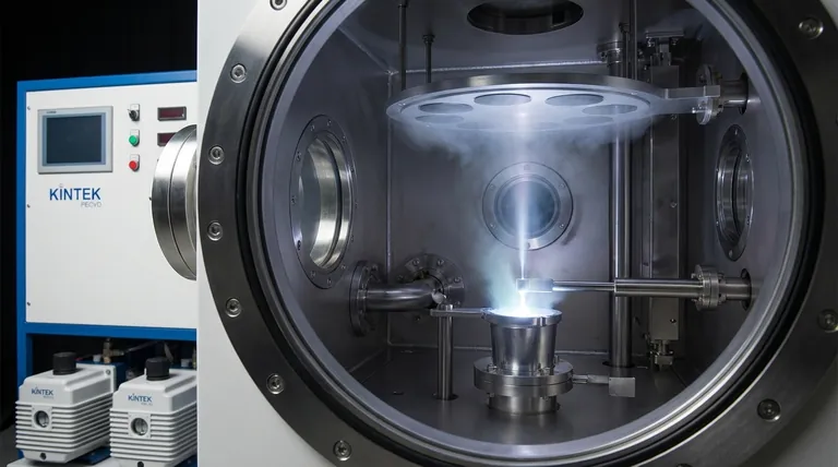
In the context of material science, the mechanism of evaporation is a process where thermal energy is used to convert a solid or liquid source material into a gas, which then condenses onto a surface to form a thin film. The most precise and widely used industrial method is electron beam (e-beam) evaporation. This technique uses a focused beam of high-energy electrons within a vacuum to heat a source material, causing it to vaporize and deposit an exceptionally pure coating onto a target substrate.
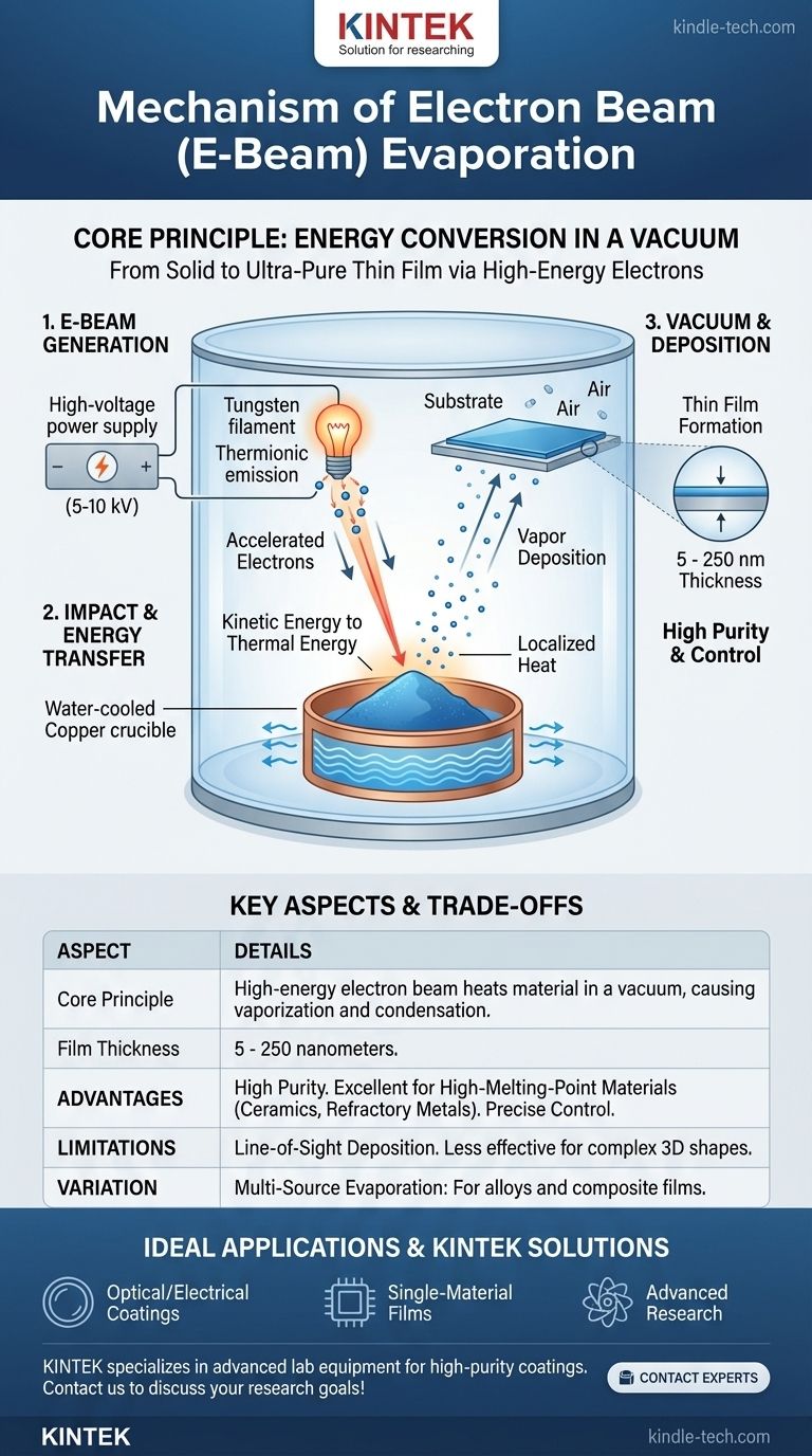
The fundamental mechanism is a direct energy conversion. E-beam evaporation transforms the high kinetic energy of electrons into intense, localized heat. This heat forces a source material to vaporize in a vacuum, allowing the resulting gas to travel and condense as a solid, ultra-pure thin film on a cooler surface.
The Core Principle: Energy in a Vacuum
The entire process hinges on precisely controlling energy transfer within a highly controlled environment. Each step is critical to achieving the desired outcome.
Step 1: Generating the Electron Beam
An electric current, typically between five and ten kilovolts (kV), is passed through a tungsten filament. This heats the filament to an extreme temperature, causing it to release electrons through a process called thermionic emission.
These electrons are then accelerated and focused into a narrow, high-energy beam.
Step 2: Impact and Energy Transfer
The high-energy electron beam is directed onto the source material, which is held in a water-cooled copper crucible. This cooling is crucial, as it ensures only the target material is heated, preventing the container itself from melting or contaminating the process.
Upon impact, the kinetic energy of the electrons is instantly converted into thermal energy, generating intense, localized heat that melts and then evaporates the source material into a vapor phase.
Step 3: The Importance of the Vacuum
This entire process occurs inside a high-vacuum chamber. The vacuum is essential for two reasons: it prevents the hot tungsten filament from oxidizing, and it removes other gas molecules that could react with the evaporated material.
This ensures the vapor travels unimpeded to the substrate, resulting in a film of exceptionally high purity.
From Vapor to Solid Film: The Deposition Process
Once the material has been converted into a gas, the final step is to precisely control its condensation into a solid film.
How the Film Forms
The vaporized particles travel in a straight line from the source toward the substrate, which is strategically positioned above the crucible.
Because the substrate is much cooler than the vapor, the particles condense upon contact, transitioning back into a solid state and forming a thin, uniform film.
Achieving Precise Thickness and Purity
The thickness of the resulting film, typically between 5 and 250 nanometers, is controlled by managing the power of the electron beam and the duration of the deposition.
This process alters the surface properties of the substrate (such as its optical or electrical characteristics) without affecting its underlying dimensional accuracy.
Understanding the Trade-offs
While powerful, e-beam evaporation is not a universal solution. Understanding its advantages and limitations is key to using it effectively.
Advantage: High Purity and Control
The combination of a high vacuum and localized heating makes this method ideal for producing films with minimal contamination. It offers exceptional control over deposition rate and film thickness.
Advantage: High-Melting-Point Materials
The intense heat generated by the electron beam makes it one of the few methods capable of evaporating materials with very high melting points, such as ceramics and refractory metals.
Limitation: Line-of-Sight Deposition
Because the vapor travels in a straight line, it can be difficult to uniformly coat complex, three-dimensional shapes. Areas not in the direct "line of sight" of the source will receive little to no coating.
Variation: Multi-Source Evaporation
For creating alloy or composite films, systems can be equipped with multiple electron beam sources. By controlling the evaporation rate from each source independently, engineers can deposit films with highly customized compositions.
Making the Right Choice for Your Goal
Selecting the correct deposition method depends entirely on the desired properties of your final product.
- If your primary focus is creating highly pure, single-material optical or electrical coatings: E-beam evaporation is an ideal choice due to its precise control and minimal contamination.
- If your primary focus is coating complex 3D shapes or deep trenches uniformly: You should consider alternative methods like sputtering or atomic layer deposition, which offer better coverage on non-flat surfaces.
- If your primary focus is developing novel alloys or composite thin films: A multi-source e-beam evaporation system provides the necessary flexibility to co-deposit different materials simultaneously.
Ultimately, understanding this mechanism empowers you to select the most effective deposition technique to achieve your specific material and application goals.
Summary Table:
| Key Aspect | Details |
|---|---|
| Core Principle | High-energy electron beam heats material in a vacuum, causing it to vaporize and condense on a substrate. |
| Typical Film Thickness | 5 - 250 nanometers |
| Key Advantage | High purity, excellent for high-melting-point materials like ceramics and refractory metals. |
| Key Limitation | Line-of-sight deposition; less effective for complex 3D shapes. |
| Ideal For | Highly pure optical/electrical coatings, single-material films. |
Ready to achieve superior thin film deposition in your lab?
KINTEK specializes in advanced lab equipment, including evaporation systems, to help you create high-purity coatings for your most demanding material science applications. Our expertise ensures you get the right solution for precise control over film thickness and composition.
Contact our experts today to discuss how our solutions can enhance your research and development!
Visual Guide
Related Products
- Electron Beam Evaporation Coating Tungsten Crucible and Molybdenum Crucible for High Temperature Applications
- Electron Beam Evaporation Coating Oxygen-Free Copper Crucible and Evaporation Boat
- Electron Beam Evaporation Coating Gold Plating Tungsten Molybdenum Crucible for Evaporation
- Electron Beam Evaporation Coating Conductive Boron Nitride Crucible BN Crucible
- E Beam Crucibles Electron Gun Beam Crucible for Evaporation
People Also Ask
- What is the current of e-beam evaporation? A Guide to High-Purity Thin Film Deposition
- What materials are used in electron beam evaporation? Master High-Purity Thin Film Deposition
- What is the process of e-beam coating? Achieve High-Purity, Precise Thin Films for Your Lab
- What is the deposition rate of e-beam evaporation? Control Thin Film Quality and Speed
- What is e-beam evaporation used for? Precision Coating for Optics, Aerospace & Electronics


