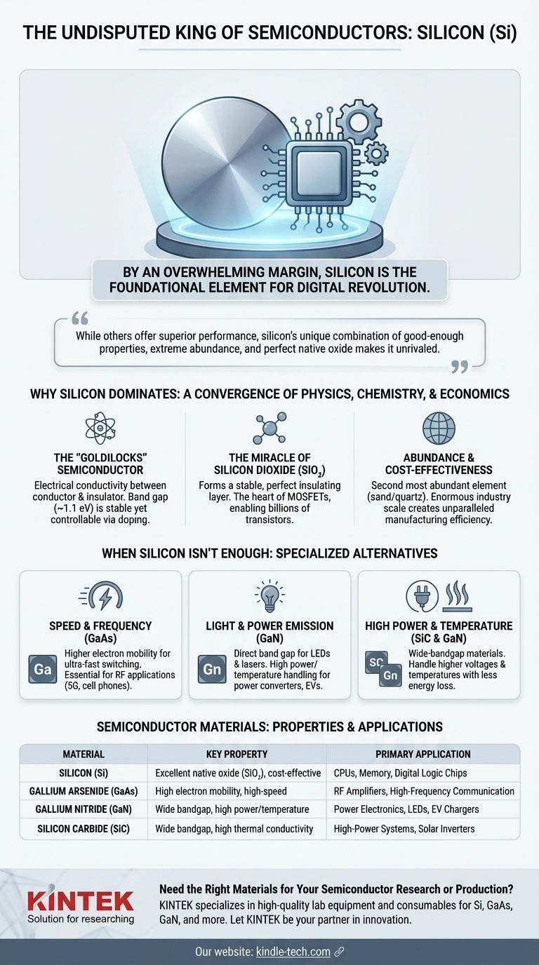
By an overwhelming margin, the most commonly used material in the semiconductor industry is silicon (Si). It is the foundational element for virtually all modern integrated circuits, from the complex processors in our computers and smartphones to the memory chips that store our data. The entire digital revolution of the past 60 years has been built, quite literally, on this single element.
While other materials offer superior performance in specific areas, silicon's unique combination of good-enough electronic properties, extreme abundance, and the ability to form a perfect, stable insulator makes it the unrivaled and most cost-effective choice for mass-produced electronics.

Why Silicon Dominates the Industry
To understand the modern world is to understand why silicon became the bedrock of electronics. Its dominance is not accidental; it stems from a convergence of physics, chemistry, and economics that no other material has been able to match on a global scale.
The "Goldilocks" Semiconductor
Silicon is a semiconductor, meaning its electrical conductivity sits between that of a conductor (like copper) and an insulator (like glass). This intermediate state is crucial.
Its band gap—the energy required to excite an electron into a conductive state—is approximately 1.1 electron volts (eV). This value is in a "just right" zone, making it stable at room temperature but easy enough to control with a process called doping, where impurities are intentionally added.
The Miracle of Silicon Dioxide (SiO₂)
This is arguably the single most important reason for silicon's dominance. When exposed to oxygen, silicon forms a thin, uniform, and exceptionally stable layer of silicon dioxide (SiO₂), which is an excellent electrical insulator.
This native oxide layer is the heart of the MOSFET (Metal-Oxide-Semiconductor Field-Effect Transistor), the microscopic switch that is the fundamental building block of all digital chips. No other semiconductor material forms such a high-quality, reliable insulating layer so easily, making the fabrication of billions of transistors on a single chip possible.
Abundance and Cost-Effectiveness
Silicon is the second most abundant element in the Earth's crust, found everywhere in the form of sand and quartz. This makes the raw material incredibly inexpensive.
While refining sand into the ultra-pure, single-crystal silicon wafers used in manufacturing is a complex process, the enormous scale of the industry has made it remarkably cost-effective. Decades of investment have created a manufacturing ecosystem around silicon that is unparalleled in its sophistication and efficiency.
Understanding the Trade-offs: When Silicon Isn't Enough
Despite its dominance, silicon is not the perfect material for every application. For specialized tasks requiring higher speed, power, or light emission, engineers turn to other materials.
The Need for Speed: Compound Semiconductors
Materials like Gallium Arsenide (GaAs) offer significantly higher electron mobility than silicon. This means electrons can move through them much faster, enabling transistors to switch at extremely high frequencies.
This property makes GaAs essential for radio-frequency (RF) applications, such as power amplifiers in cell phones and high-speed communication systems where silicon would be too slow.
Emitting Light and Handling Power
Silicon has an "indirect" band gap, which makes it extremely inefficient at converting electricity into light. For applications like LEDs and lasers, materials with a "direct" band gap, such as Gallium Nitride (GaN), are required.
Furthermore, for high-power and high-temperature electronics, wide-bandgap semiconductors like GaN and Silicon Carbide (SiC) are rapidly replacing silicon. Their ability to handle higher voltages and temperatures with less energy loss is critical for power converters, electric vehicle inverters, and the future of the power grid.
The Manufacturing Hurdle
While these compound semiconductors offer superior performance, they are far more difficult and expensive to produce than silicon. They often require complex crystal growth methods, and they do not benefit from a perfect native oxide like silicon does. This confines their use to applications where their specific advantages justify the higher cost.
Making the Right Choice for Your Goal
The choice of semiconductor material is always driven by the specific performance requirements and economic constraints of the application.
- If your primary focus is cost-effective, large-scale digital logic (CPUs, GPUs, memory): Silicon is and will remain the undisputed choice due to its mature ecosystem and perfectly balanced properties.
- If your primary focus is high-frequency radio or optical devices (LEDs, 5G hardware): Compound semiconductors like Gallium Arsenide (GaAs) and Gallium Nitride (GaN) are necessary for their superior speed and light-emitting capabilities.
- If your primary focus is high-power, high-temperature electronics (EV chargers, solar inverters): Wide-bandgap semiconductors like Silicon Carbide (SiC) and Gallium Nitride (GaN) are the superior choice, offering efficiency and durability beyond silicon's limits.
Understanding these material distinctions reveals why our digital world is built on a foundation of sand, yet relies on more exotic materials to push the boundaries of performance.
Summary Table:
| Material | Key Property | Primary Application |
|---|---|---|
| Silicon (Si) | Excellent native oxide (SiO₂), cost-effective | CPUs, Memory, Digital Logic Chips |
| Gallium Arsenide (GaAs) | High electron mobility, high-speed | RF Amplifiers, High-Frequency Communication |
| Gallium Nitride (GaN) | Wide bandgap, high power/temperature | Power Electronics, LEDs, EV Chargers |
| Silicon Carbide (SiC) | Wide bandgap, high thermal conductivity | High-Power Systems, Solar Inverters |
Need the Right Materials for Your Semiconductor Research or Production?
Choosing the correct semiconductor material is critical for the performance and efficiency of your project. At KINTEK, we specialize in providing high-quality lab equipment and consumables tailored to the precise needs of semiconductor development and manufacturing.
Whether you are working with silicon wafers, compound semiconductors like GaAs and GaN, or require specialized tools for high-temperature processing, KINTEK has the expertise and products to support your work.
Let KINTEK be your partner in innovation. Contact our experts today to discuss how our solutions can help you achieve superior results and push the boundaries of your semiconductor applications.
Visual Guide
Related Products
- Silicon Carbide (SIC) Ceramic Sheet Wear-Resistant Engineering Advanced Fine Ceramics
- Silicon Carbide (SIC) Ceramic Sheet Flat Corrugated Heat Sink for Engineering Advanced Fine Ceramics
- Silicon Carbide (SIC) Ceramic Plate for Engineering Advanced Fine Ceramics
- Precision Machined Silicon Nitride (SiN) Ceramic Sheet for Engineering Advanced Fine Ceramics
- Silicon Carbide SiC Thermal Heating Elements for Electric Furnace
People Also Ask
- What are the uses of silicon carbide ceramics in different industries? Master Extreme Performance in Aerospace, Semiconductors & More
- What are the properties of SiC? Unlock High-Temperature, High-Frequency Performance
- What are the applications of silicon carbide? From Abrasives to High-Tech Semiconductors
- What are the common uses of silicon carbide? Unlock Extreme Performance in Harsh Environments
- Why is silicon carbide more efficient? Unlock Higher Power Density with SiC's Superior Material Properties