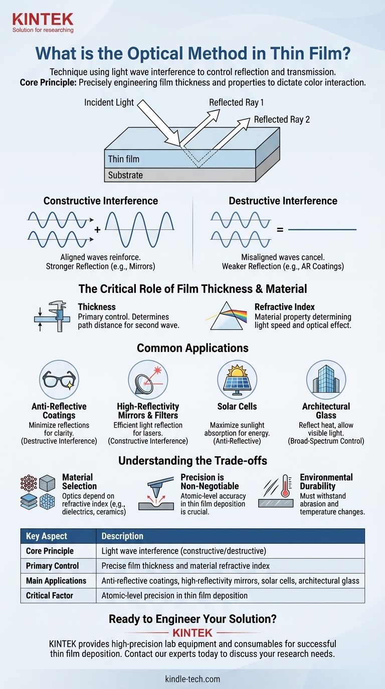
The optical method in thin films is a technique that uses the principle of light wave interference to control how light is reflected or transmitted. When light hits a thin film, some reflects off the top surface while the rest enters the film and reflects off the bottom surface. These two reflected light waves then interact, either reinforcing each other to increase reflection or canceling each other out to reduce it.
At its core, the optical method isn't about the film itself, but about precisely engineering the film's thickness and material properties. By doing so, you can dictate which specific colors (wavelengths) of light are reflected or passed through, giving you precise control over the optical properties of a surface.
The Core Principle: Manipulating Light with Interference
To understand the power of optical thin films, you must first grasp the physics of light wave interference. This single principle is the foundation for all of its applications.
How Light Interacts with a Thin Film
When a light wave strikes a thin film, it splits. A portion of the wave reflects immediately from the top surface. The remaining portion travels through the film, hits the bottom surface, and then reflects back up.
The optical method hinges on controlling the interaction between these two separate reflected waves.
Constructive vs. Destructive Interference
The key is the relationship between the two reflected waves.
- Constructive Interference: If the waves exiting the film are aligned (in-phase), their amplitudes add together. This makes the reflection for that specific color of light stronger. This is used to create highly reflective mirrors.
- Destructive Interference: If the waves are perfectly misaligned (out-of-phase), they cancel each other out. This makes the reflection for that color weaker, allowing more light to pass through. This is the principle behind anti-reflective coatings.
The Critical Role of Film Thickness
The thickness of the film is the primary control knob. It determines the path distance the second light wave has to travel before it exits and interferes with the first wave.
By precisely controlling this thickness—often down to a fraction of a wavelength of light—engineers can ensure that specific colors undergo either constructive or destructive interference.
Common Applications of the Optical Method
This simple principle of interference is leveraged across numerous high-tech industries to solve critical optical challenges.
Anti-Reflective Coatings
This is the most common application. By applying a thin film of a carefully chosen material and thickness to a lens (like on eyeglasses or a camera), reflections are minimized through destructive interference. This increases light transmission, reduces glare, and improves image clarity.
High-Reflectivity Mirrors and Filters
Conversely, constructive interference can be used to create highly efficient mirrors. By stacking multiple layers of thin films, engineers can design mirrors that reflect more than 99% of light, but only for a very specific range of colors. These are essential components in lasers and advanced optical instruments.
Solar Cells and Architectural Glass
In solar cells, thin films are used as anti-reflective coatings to ensure the maximum amount of sunlight enters the cell to be converted into electricity. In modern architecture, sophisticated thin films on glass can reflect infrared light (heat) while allowing visible light to pass through, significantly improving a building's energy efficiency.
Understanding the Trade-offs
While powerful, the optical method is not without its complexities. The performance of a thin film is highly dependent on precision and material science.
Material Selection is Crucial
The optical properties of a thin film depend on its refractive index, a measure of how much it slows down light. Different materials, such as dielectrics, ceramics, or nitrides, have different refractive indices. The choice of material is just as critical as the film's thickness in determining the final optical effect.
Precision is Non-Negotiable
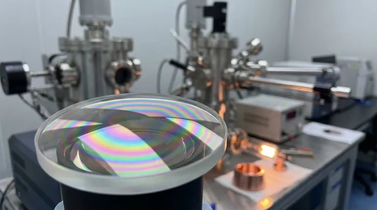
The manufacturing process, known as thin film deposition, requires atomic-level precision. A deviation of just a few nanometers in film thickness can completely alter which colors are reflected or transmitted, rendering the coating ineffective for its intended purpose.
Environmental Durability
An optical coating is often the outermost surface of a product. It must be durable enough to withstand abrasion, temperature changes, and humidity without degrading its optical performance. Balancing perfect optical properties with real-world resilience is a constant engineering challenge.
Making the Right Choice for Your Goal
The design of an optical thin film is entirely driven by the desired outcome. The same principle of interference is simply tuned to achieve opposite effects.
- If your primary focus is maximum light transmission (e.g., lenses, displays, solar panels): Your design must create destructive interference for visible light, resulting in an anti-reflective coating.
- If your primary focus is selective reflection (e.g., laser mirrors, color filters): Your design must create constructive interference for specific target wavelengths.
- If your primary focus is broad-spectrum control (e.g., energy-efficient windows): You will likely need a complex stack of multiple thin film layers, each designed to interfere with a different portion of the light spectrum.
By mastering the principle of light wave interference, thin film technology allows us to precisely engineer the very behavior of light.
Summary Table:
| Key Aspect | Description |
|---|---|
| Core Principle | Light wave interference (constructive/destructive) |
| Primary Control | Precise film thickness and material refractive index |
| Main Applications | Anti-reflective coatings, high-reflectivity mirrors, solar cells, architectural glass |
| Critical Factor | Atomic-level precision in thin film deposition |
Ready to Engineer Your Optical Thin Film Solution?
KINTEK specializes in providing the high-precision lab equipment and consumables essential for successful thin film deposition. Whether you are developing anti-reflective coatings, laser mirrors, or energy-efficient glass, our expertise ensures you achieve the exact thickness and material properties required for optimal light interference.
Contact our experts today to discuss how KINTEK can support your laboratory's thin film research and production needs.
Visual Guide