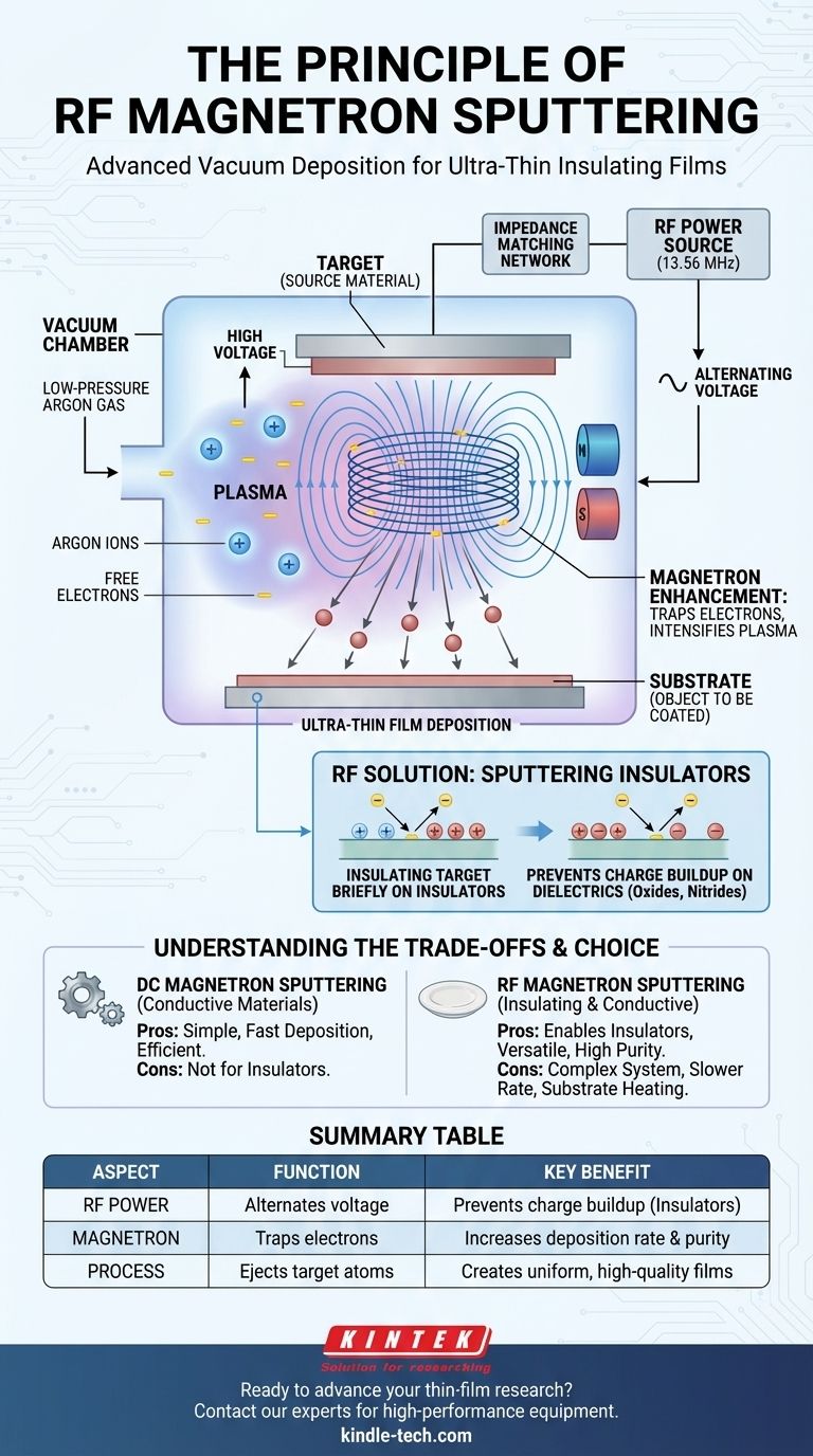
At its core, RF magnetron sputtering is a vacuum deposition technique used to create ultra-thin films. It uses an alternating, radio-frequency (RF) power source to generate a plasma and a magnetic field to intensify it. This intensified plasma bombards a source material (the "target"), knocking atoms loose that then travel and deposit as a uniform coating onto a substrate. The critical advantage of using an RF source is its ability to deposit insulating materials, which is impossible with simpler direct-current (DC) methods.
The central principle isn't just about bombarding a target; it's about sustaining that bombardment on any type of material. RF magnetron sputtering solves this by combining a magnetic field to create a dense plasma with an alternating electric field that prevents electrical charge from building up on insulating targets, enabling the deposition of a vast range of advanced materials.
The Core Mechanism: From Plasma to Film
To understand the "RF" and "magnetron" aspects, we must first understand the basic sputtering process. It unfolds in a highly controlled vacuum environment.
Creating the Plasma Environment
The process begins inside a vacuum chamber that is filled with a low-pressure inert gas, almost always argon. A high voltage is applied, which strips electrons from the argon atoms. This creates a plasma, an energized gas consisting of positively charged argon ions and free electrons.
The Bombardment Process
The target, which is made of the material you wish to deposit, is given a negative electrical potential. This attracts the positively charged argon ions from the plasma, causing them to accelerate and collide with the target at high speed. This is a purely physical process, often compared to a microscopic sandblaster.
Deposition onto the Substrate
The energy from these ion collisions is forceful enough to knock atoms or molecules completely free from the target material. These ejected particles travel through the vacuum chamber and land on the substrate (the object being coated), gradually building up a thin, uniform film.
The "Magnetron" Enhancement: Efficiency and Control
Standard sputtering is slow and inefficient. The addition of a magnetic field—the "magnetron" part of the name—dramatically improves the process.
Trapping Electrons
Powerful magnets are placed behind the target. This magnetic field traps the free electrons from the plasma, forcing them into a spiral path directly in front of the target's surface.
Increasing Ionization Efficiency
By trapping electrons near the target, their path length is greatly increased. This means they are far more likely to collide with and ionize neutral argon gas atoms. The result is a much denser, more intense plasma concentrated where it's most needed.
The Result: Faster and Denser Films
This high-density plasma generates significantly more argon ions to bombard the target. This leads to a much faster deposition rate and allows the process to operate at lower gas pressures, resulting in higher-purity films.
The "RF" Solution: Sputtering Insulators
This is the most critical concept. While a constant negative voltage (DC) works for conductive targets, it fails completely for insulators.
The Challenge with Insulating Targets
If you use a DC power source on an insulating target (like an oxide or nitride), the incoming positive argon ions quickly accumulate on the surface. Since the target is an insulator, this positive charge cannot dissipate. This effect, known as "target poisoning" or charging, repels further positive ions and effectively stops the sputtering process within seconds.
How the Alternating Field Works
An RF power source solves this by rapidly alternating the target's voltage (typically at 13.56 MHz).
- During the negative half-cycle, positive argon ions are attracted to the target, and sputtering occurs as normal.
- During the brief positive half-cycle, the target attracts electrons from the plasma. These electrons instantly neutralize the positive charge built up during the negative cycle.
This rapid clearing of the positive charge allows the sputtering process to continue indefinitely, making it the standard method for depositing dielectric and insulating films.
Understanding the Trade-offs
While powerful, RF sputtering is not without its complexities. Objectively assessing these is key to its proper application.
System Complexity
RF systems are more complex and expensive than their DC counterparts. They require a dedicated RF power supply and an impedance matching network to ensure efficient power transfer from the supply to the plasma, which can be difficult to tune.
Deposition Rates
For materials that are electrically conductive (metals), DC magnetron sputtering is almost always faster and more efficient. RF is typically reserved for materials where DC is not a viable option.
Substrate Heating
The high-density plasma and electron activity inherent in RF sputtering can impart a significant amount of heat to the substrate. This can be a limiting factor when coating temperature-sensitive materials like polymers.
Making the Right Choice for Your Goal
The decision between RF and other methods is dictated entirely by the material you intend to deposit.
- If your primary focus is depositing conductive materials (like metals): DC magnetron sputtering is often preferred for its higher deposition rates and simpler setup.
- If your primary focus is depositing insulating materials (like oxides or nitrides): RF magnetron sputtering is the essential and standard method, as it overcomes the critical charge buildup issue.
- If your primary focus is creating complex, multi-layer films with both types of materials: A system equipped with both RF and DC capabilities offers the most process versatility.
Ultimately, understanding the role of the alternating field is the key to leveraging RF sputtering for advanced material deposition.
Summary Table:
| Aspect | Function | Key Benefit |
|---|---|---|
| RF Power | Alternates target voltage to prevent charge buildup | Enables sputtering of insulating materials (oxides, nitrides) |
| Magnetron | Traps electrons with a magnetic field to intensify plasma | Increases deposition rate and film purity |
| Process | Physically ejects target atoms via ion bombardment | Creates uniform, high-quality thin films |
Ready to advance your thin-film research with precision equipment?
KINTEK specializes in providing high-performance lab equipment and consumables for advanced material deposition. Whether you are developing next-generation semiconductors, optical coatings, or complex multi-layer films, our RF magnetron sputtering solutions offer the reliability and control your laboratory needs.
Contact our experts today to discuss how we can support your specific application and help you achieve superior deposition results.
Visual Guide
Related Products
People Also Ask
- What is plasma chemical vapor deposition? A Low-Temperature Thin Film Coating Solution
- Why is a Matching Network Indispensable in RF-PECVD for Siloxane Films? Ensure Stable Plasma and Uniform Deposition
- What is plasma enhanced chemical vapour deposition PECVD used for? Enable Low-Temp Thin Films for Electronics & Solar
- What is the role of RF-PECVD in VFG preparation? Mastering Vertical Growth and Surface Functionality
- What is plasma CVD? Unlock Low-Temperature Thin Film Deposition for Sensitive Materials
