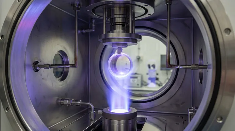
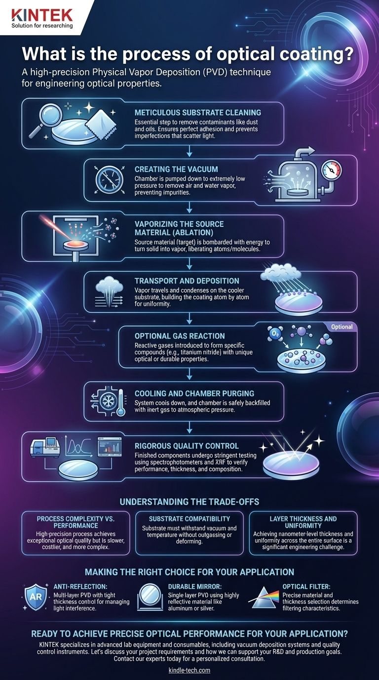
At its core, the optical coating process is a high-precision technique for depositing exceptionally thin layers of material onto an optical component, like a lens or mirror. This is most commonly achieved through Physical Vapor Deposition (PVD) inside a vacuum chamber. The fundamental steps involve meticulously cleaning the component (substrate), creating a high vacuum, vaporizing a source material, and allowing it to condense onto the substrate in ultra-thin, controlled layers.
The challenge of optical coating isn't simply applying a layer; it's about engineering the optical properties of a surface at a near-atomic level. The entire process is designed to create pure, uniform films with thicknesses measured in nanometers to precisely control how light is reflected, transmitted, or filtered.
The Foundational Stages: Preparation and Environment
Before any material can be deposited, the substrate and its environment must be perfect. Any deviation at this stage will compromise the final quality of the coating.
Stage 1: Meticulous Substrate Cleaning
The first and most critical step is cleaning the substrate. Any microscopic contaminants, such as dust, oils, or residues, will prevent the coating from adhering correctly.
This failure in adhesion creates imperfections that can scatter light and degrade optical performance, rendering the component useless for high-precision applications.
Stage 2: Creating the Vacuum
The cleaned components are loaded into a vacuum chamber, which is then pumped down to an extremely low pressure.
This vacuum is essential because it removes air and water vapor. These particles would otherwise collide with the coating material during its transit, causing impurities and a non-uniform film.
The Heart of the Process: Material Deposition
This phase is where the coating is actually formed. It is a sequence of physical processes that are controlled with immense precision.
Stage 3: Vaporizing the Source Material (Ablation)
Inside the chamber, a source material, known as a target, is bombarded with energy to turn it from a solid into a vapor.
This is often accomplished using methods like an electron beam or an electrical arc to strike the target, liberating individual atoms or molecules. This is the "Physical Vapor" part of PVD.
Stage 4: Transport and Deposition
The vaporized material travels in a straight line through the vacuum and condenses on the cooler surface of the optical components.
This process builds the coating atom by atom, creating an exceptionally thin and uniform film. For complex coatings, this is repeated with different materials to build up a stack of multiple layers.
Stage 5: Optional Gas Reaction
In some cases, a reactive gas like oxygen or nitrogen is introduced into the chamber.
The vaporized metal atoms react with this gas as they deposit onto the substrate, forming a specific compound (like titanium nitride or silicon dioxide) with unique optical or durable properties.
Ensuring Performance: Final Steps and Quality Control
A coating is only as good as its measured performance. The process concludes with verification and a return to normal atmospheric conditions.
Stage 6: Cooling and Chamber Purging
Once the deposition is complete, the system is allowed to cool. The chamber is then carefully backfilled with an inert gas, like argon, to safely bring it back to atmospheric pressure.
Stage 7: Rigorous Quality Control
Finished components undergo stringent testing. Each batch is inspected to ensure consistency and performance.
Specialized instruments like spectrophotometers are used to measure how the coating reflects and transmits light, while an X-ray fluorescent (XRF) machine can verify the film's thickness and composition.
Understanding the Trade-offs
While powerful, the optical coating process involves inherent complexities and limitations that must be managed.
Process Complexity vs. Performance
This is a highly engineered and often slow process. The exceptional optical performance, durability, and precision achieved come at a higher cost and complexity compared to standard coating methods.
Substrate Compatibility
The substrate material must be able to withstand the vacuum and temperature changes inside the chamber without deforming or releasing its own gases ("outgassing"), which would contaminate the process.
Layer Thickness and Uniformity
Achieving a perfectly uniform coating thickness, especially on a curved lens, is a significant engineering challenge. The entire process relies on tight control over temperature, pressure, and deposition rate to ensure every part of the optic performs identically.
Making the Right Choice for Your Application
The specific parameters of the coating process are tailored to the desired optical outcome.
- If your primary focus is high-performance anti-reflection: You need a multi-layer PVD process with extremely tight thickness control to manage light interference across different wavelengths.
- If your primary focus is creating a durable mirror: A single-layer PVD process using a highly reflective material like aluminum or silver is often the most effective and direct solution.
- If your primary focus is filtering specific wavelengths of light: The choice of coating materials and the precise thickness of each layer are paramount, as these factors directly determine the filter's cut-off and pass-band characteristics.
Understanding this process of atomic-level engineering is the first step toward specifying a coating that meets your exact performance requirements.
Summary Table:
| Stage | Key Action | Purpose |
|---|---|---|
| 1. Preparation | Meticulous Substrate Cleaning | Ensures perfect adhesion and eliminates light-scattering contaminants. |
| 2. Environment | Creating a High Vacuum | Removes air and vapor to prevent impurities and ensure a uniform film. |
| 3. Deposition | Vaporizing the Source Material (Ablation) | Liberates atoms/molecules from a target using an electron beam or arc. |
| 4. Deposition | Transport and Condensation | Builds the coating atom-by-atom on the substrate for ultra-thin layers. |
| 5. (Optional) | Introducing Reactive Gas | Forms compounds like titanium nitride for specific optical/durable properties. |
| 6. Finalization | Cooling and Chamber Purging | Safely returns the system to atmospheric pressure with an inert gas. |
| 7. Verification | Rigorous Quality Control | Uses spectrophotometers and XRF to verify performance, thickness, and composition. |
Ready to achieve precise optical performance for your application?
The intricate process of optical coating requires reliable, high-performance equipment to ensure purity, uniformity, and exact thickness control. KINTEK specializes in advanced lab equipment and consumables for laboratory needs, including vacuum deposition systems and quality control instruments.
We can provide the tools and expertise to help you develop high-performance anti-reflective coatings, durable mirrors, or precise optical filters. Let's discuss your project requirements and how we can support your R&D and production goals.
Contact our experts today for a personalized consultation.
Visual Guide
Related Products
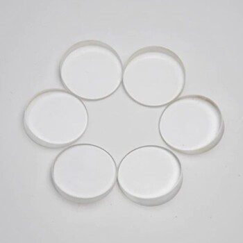
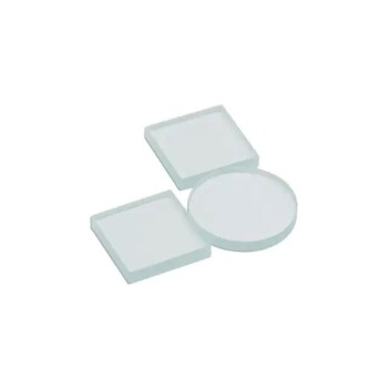
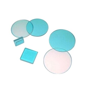
- Infrared Transmission Coating Sapphire Sheet Substrate Window
- Optical Window Glass Substrate Wafer Single Double Sided Coated K9 Quartz Sheet
- 400-700nm Wavelength Anti Reflective AR Coating Glass
- MgF2 Magnesium Fluoride Crystal Substrate Window for Optical Applications
- Infrared Thermal Imaging Temperature Measurement Double-Sided Coated Germanium Ge Lens
People Also Ask
- What do optical coatings do? Control Light for Superior Optical Performance
- How do cooling jackets or heat exchangers contribute to the stability of glycerol conversion? Master Thermal Management
- Is Sputter Tint good? Premium Heat Rejection & Long-Term Durability Explained
- What is the optical coating? Master Light Control for Superior Optical Performance
- What is organic thin film? A Guide to Engineered Molecular Layers for Advanced Tech