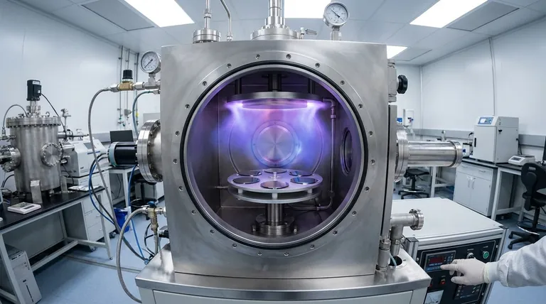
In essence, sputtering is a highly controlled, physical process for depositing exceptionally thin layers of material. It functions like a sandblaster at the atomic scale, using energized gas ions instead of sand to chip away individual atoms from a source material. These ejected atoms then travel through a vacuum and evenly coat a target object, or substrate, forming a new, high-performance surface.
Sputtering is a specific type of Physical Vapor Deposition (PVD) that creates thin films with superior adhesion and uniformity. It works by bombarding a source material with plasma in a vacuum, physically knocking atoms loose and redepositing them onto a substrate.
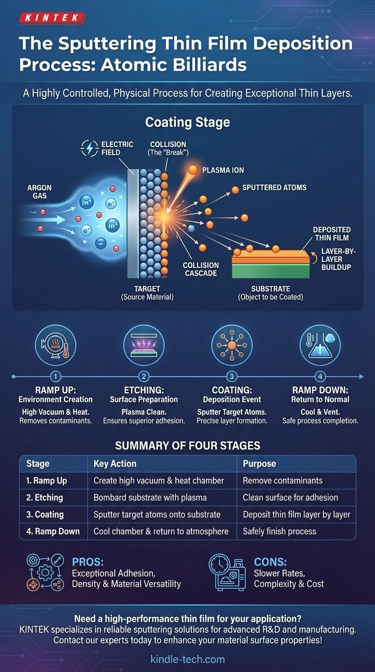
The Core Principle: A Billiards Game at the Atomic Scale
To truly understand sputtering, it's best to visualize it as a game of atomic billiards taking place inside a vacuum chamber. This environment is critical because it removes other gas molecules that could interfere with the process.
The Target (The Rack of Balls)
The process begins with the target, which is a block or plate made of the pure material you wish to deposit as a coating. This could be a metal, an oxide, or a complex compound.
The Plasma (The Cue Ball)
To start the process, a small amount of an inert gas, typically Argon, is introduced into the vacuum chamber. An electric field is then applied, which energizes the gas and strips electrons from the Argon atoms, creating a plasma—a cloud of positively charged Argon ions.
The Collision (The "Break")
A negative voltage is applied to the target material. This causes the positive Argon ions from the plasma to accelerate violently and slam into the target surface.
This high-energy bombardment sets off a collision cascade. The impacting ion transfers its momentum to the atoms in the target, which in turn hit other atoms, much like a powerful break shot in billiards.
The Deposition (The Result)
Some atoms near the target's surface gain enough energy from these collisions to be ejected, or "sputtered," away from the target. These dislodged atoms travel through the vacuum and land on the substrate (the component being coated), building up layer by layer to form a dense, uniform, and highly adherent thin film.
The Four Stages of a Sputtering Cycle
A typical industrial sputtering process follows a clear, four-stage sequence to ensure quality and repeatability.
Stage 1: Ramp Up (Creating the Environment)
The substrate and target are placed inside the vacuum chamber. Air and contaminants are pumped out to create a high-vacuum environment. The chamber may also be heated to a specific process temperature.
Stage 2: Etching (Preparing the Surface)
Before coating, the substrate itself is often cleaned using a similar plasma process. This cathodic etching removes any microscopic surface contamination, ensuring the final film has the strongest possible bond to the substrate.
Stage 3: Coating (The Deposition Event)
This is the main stage where the target material is bombarded by the plasma and the ejected atoms are deposited onto the substrate, as described in the process above. This step is carefully timed to achieve the precise film thickness required.
Stage 4: Ramp Down (Returning to Normal)
Once the desired thickness is achieved, the power supplies are turned off, and the chamber is allowed to cool. It is then slowly returned to normal atmospheric pressure, and the newly coated components can be removed.
Understanding the Trade-offs
Sputtering is a powerful and widely used technique, but like any engineering process, it involves specific advantages and limitations.
Pro: Exceptional Adhesion and Film Density
The sputtered atoms arrive at the substrate with significant kinetic energy. This energy helps them form a very strong mechanical and chemical bond with the surface, resulting in a dense and durable film that is difficult to peel or flake off.
Pro: Versatility of Materials
Sputtering can be used to deposit virtually any material, including metals, ceramics, and complex alloys. Because it's a physical and not a chemical process, it can deposit compounds without altering their chemical composition from the target to the substrate.
Con: Slower Deposition Rates
Compared to some other methods like thermal evaporation, sputtering is generally a slower process. This can make it less suitable for applications requiring very thick coatings or extremely high throughput.
Con: Complexity and Cost
Sputtering systems require high-vacuum chambers, sophisticated power supplies, and cooling systems. This makes the initial equipment investment more significant than simpler coating methods.
Making the Right Choice for Your Goal
Selecting the right deposition technique depends entirely on the required properties of the final film.
- If your primary focus is material adhesion and film density: Sputtering is a superior choice due to the high kinetic energy of the deposited atoms creating a stronger bond.
- If your primary focus is depositing complex alloys or compounds: Sputtering excels because it reliably preserves the chemical ratio (stoichiometry) from the target to the film.
- If your primary focus is high-speed, bulk coating of simple metals: You might consider an alternative PVD method like thermal evaporation, which often provides higher deposition rates.
Ultimately, understanding the sputtering process empowers you to select the most effective method for modifying a material's surface to meet precise performance requirements.
Summary Table:
| Stage | Key Action | Purpose |
|---|---|---|
| 1. Ramp Up | Create high vacuum & heat chamber | Remove contaminants, prepare environment |
| 2. Etching | Bombard substrate with plasma | Clean surface for superior film adhesion |
| 3. Coating | Sputter target atoms onto substrate | Deposit the thin film layer by layer |
| 4. Ramp Down | Cool chamber & return to atmosphere | Safely finish the process |
Need a high-performance thin film for your application? The sputtering process delivers exceptional adhesion, uniformity, and material versatility—perfect for advanced R&D and manufacturing. KINTEK specializes in lab equipment and consumables, providing reliable sputtering solutions to meet your laboratory's precise coating needs. Contact our experts today to discuss how we can enhance your material surface properties!
Visual Guide
Related Products
- Spark Plasma Sintering Furnace SPS Furnace
- Vacuum Induction Melting Spinning System Arc Melting Furnace
- Chemical Vapor Deposition CVD Equipment System Chamber Slide PECVD Tube Furnace with Liquid Gasifier PECVD Machine
- Customer Made Versatile CVD Tube Furnace Chemical Vapor Deposition Chamber System Equipment
People Also Ask
- What are the advantages of CAMI/SPS for W-Cu composite preparation? Reduce cycles from hours to seconds.
- What technical advantages does a Spark Plasma Sintering (SPS) furnace offer for LZP ceramics? Enhance Ionic Conductivity
- What is SPS sintering method? A Guide to High-Speed, High-Performance Material Fabrication
- What is the theory of spark plasma sintering? A Guide to Rapid, Low-Temperature Densification
- What is the pressure for spark plasma sintering? A Guide to Optimizing SPS Parameters


