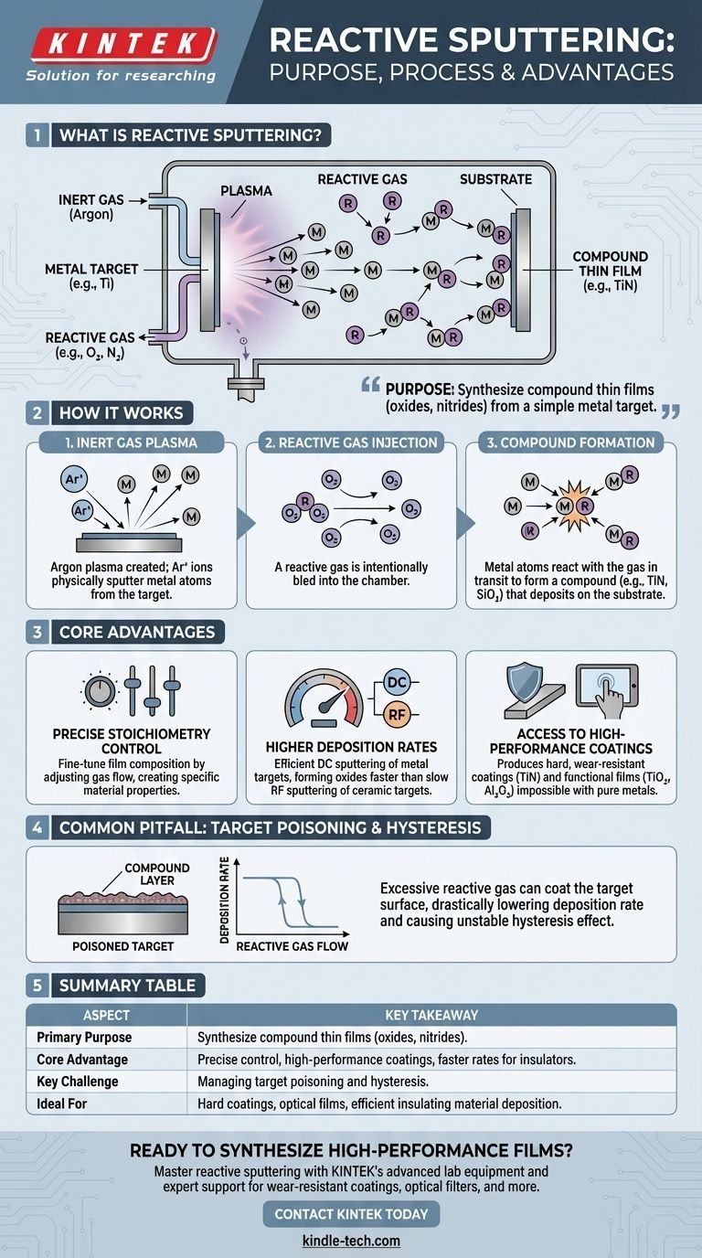
The primary purpose of reactive sputtering is to create compound thin films, such as oxides and nitrides, by sputtering a pure metal target in the presence of a chemically reactive gas. Instead of sputtering from a complex ceramic target, this method uses a simple metal target and introduces a gas like oxygen or nitrogen into the chamber, which reacts with the sputtered metal atoms to form the desired compound on the substrate.
At its core, reactive sputtering is a technique for material synthesis. It transforms a simple, easy-to-sputter metallic target into a complex compound coating, giving you precise control over the final film's chemical composition and properties.
How Reactive Sputtering Works
The process cleverly combines the mechanics of physical sputtering with a controlled chemical reaction. This is managed by the precise introduction of two different types of gases into the vacuum chamber.
The Role of the Inert Gas
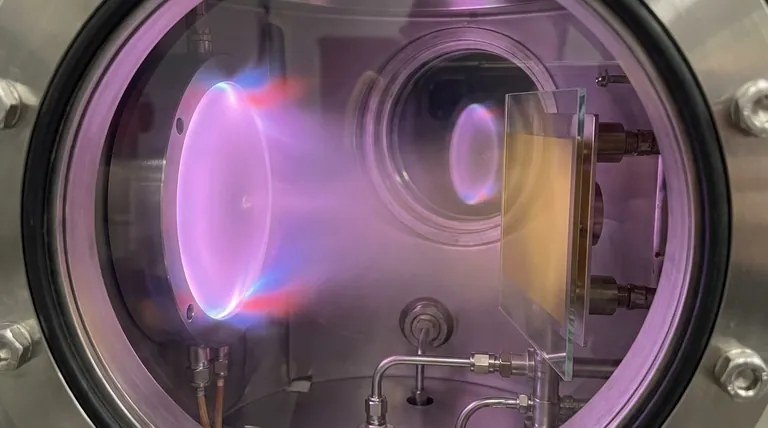
First, an inert gas like Argon (Ar) is introduced. A strong electric field energizes this gas, creating a plasma.
Positively charged Argon ions are accelerated toward the negatively charged target material (e.g., pure Titanium). These energetic ions bombard the target, physically knocking off, or "sputtering," individual atoms of the target material.
The Role of the Reactive Gas
At the same time, a second, reactive gas is carefully bled into the chamber. This is typically Oxygen (O₂) for oxides or Nitrogen (N₂) for nitrides.
This gas is the key to the transformation. It is intentionally chosen to react chemically with the freshly sputtered metal atoms.
The Formation of a Compound Film
As the metal atoms travel from the target to the substrate, they encounter and react with the molecules of the reactive gas.
This chemical reaction forms a new compound—for example, Titanium atoms reacting with Nitrogen gas to form Titanium Nitride (TiN). This compound then deposits onto the substrate, building up the desired thin film layer by layer.
The Core Advantages of This Method
Engineers and scientists choose reactive sputtering over other methods for several critical reasons, primarily revolving around control, efficiency, and material properties.
Precise Control Over Stoichiometry
The most significant advantage is the ability to fine-tune the chemical composition (stoichiometry) of the deposited film.
By carefully adjusting the flow rate of the reactive gas relative to the inert gas, you can control the exact ratio of elements in the final film. This allows for the creation of specific sub-oxides or nitrides with unique optical or electrical properties.
Higher Deposition Rates for Insulating Films
Sputtering directly from an insulating ceramic target (e.g., Aluminum Oxide) must be done with a radio frequency (RF) power supply, which is often slow.
Reactive sputtering provides a powerful alternative. You can use a highly efficient direct current (DC) power supply to sputter a pure metal target (e.g., Aluminum), which has a much higher deposition rate. The introduction of oxygen then forms the insulating Aluminum Oxide film on the substrate, combining the speed of DC sputtering with the desired ceramic outcome.
Access to High-Performance Coatings
This technique is the industry standard for producing a wide range of high-performance coatings that are impossible to create with a pure metal.
Examples include hard, wear-resistant coatings like Titanium Nitride (TiN) for cutting tools or decorative finishes, and transparent conductive oxides for touch screens and solar cells.
Common Pitfalls to Avoid: The Hysteresis Effect
While powerful, reactive sputtering has a well-known process control challenge that can frustrate inexperienced operators. The core issue is known as "target poisoning."
What is Target Poisoning?
If the flow of the reactive gas is too high, it doesn't just react with sputtered atoms in transit. It begins to react with and form a compound layer directly on the surface of the sputtering target itself.
This is called target poisoning. For example, in a process meant to create Titanium Nitride, the Titanium target itself becomes coated in a layer of TiN.
The Consequence: A Drastic Drop in Speed
The sputtering rate of a ceramic compound is dramatically lower than that of a pure metal.
When the target becomes poisoned, the overall deposition rate plummets. This creates a highly unstable process that is difficult to control and repeat.
The Hysteresis Loop
This leads to a "hysteresis" effect. As you slowly increase reactive gas flow, the deposition rate stays high until it suddenly collapses when the target poisons. If you then try to decrease the gas flow, the rate does not recover along the same path. You have to lower the gas flow significantly to clean the poison layer off the target before the rate jumps back up. This non-linear behavior makes finding a stable operating point a significant challenge.
Making the Right Choice for Your Goal
Understanding reactive sputtering allows you to select it for the right applications.
- If your primary focus is high-performance hard coatings: This is the ideal method for depositing wear-resistant nitrides and carbides (e.g., TiN, TiCN) on tools and components.
- If your primary focus is optical or electrical films: The process offers unparalleled control for creating specific oxides (e.g., SiO₂, TiO₂, Al₂O₃) used in anti-reflection coatings, filters, and insulators.
- If your primary focus is high-speed deposition of compounds: Reactive sputtering with a DC source is often the most cost-effective and efficient way to produce compound films compared to slower RF sputtering from a ceramic target.
Ultimately, reactive sputtering gives you the power to synthesize a vast library of functional materials from a small set of simple, pure metallic targets.
Summary Table:
| Aspect | Key Takeaway |
|---|---|
| Primary Purpose | To synthesize compound thin films (e.g., oxides, nitrides) by sputtering a metal target in a reactive gas atmosphere. |
| Core Advantage | Precise control over film stoichiometry and properties, enabling high-performance coatings. |
| Key Challenge | Managing the hysteresis effect and target poisoning to maintain a stable, high-rate deposition process. |
| Ideal For | Hard coatings (TiN), optical films (SiO₂), and efficient deposition of insulating materials. |
Ready to synthesize high-performance thin films for your laboratory?
Reactive sputtering is a powerful technique for creating custom compound coatings with precise properties. At KINTEK, we specialize in providing the advanced lab equipment and expert support you need to master this process.
Whether you are developing wear-resistant tool coatings, optical filters, or specialized electronic layers, our sputtering systems and consumables are designed for reliability and control.
Contact our experts today to discuss how KINTEK's solutions can help you achieve superior film quality and accelerate your research and development.
Visual Guide
Related Products
- Spark Plasma Sintering Furnace SPS Furnace
- Chemical Vapor Deposition CVD Equipment System Chamber Slide PECVD Tube Furnace with Liquid Gasifier PECVD Machine
- RF PECVD System Radio Frequency Plasma-Enhanced Chemical Vapor Deposition RF PECVD
- Customer Made Versatile CVD Tube Furnace Chemical Vapor Deposition Chamber System Equipment
- Vacuum Induction Melting Spinning System Arc Melting Furnace
People Also Ask
- What is SPS sintering method? A Guide to High-Speed, High-Performance Material Fabrication
- What are the fundamentals of spark plasma sintering process? Unlock Rapid, High-Performance Material Consolidation
- What is the process fundamentals of spark plasma sintering? Achieve Rapid, High-Density Material Consolidation
- What is the mechanism of SPS process? A Deep Dive into Rapid, Low-Temperature Sintering
- What are the advantages of CAMI/SPS for W-Cu composite preparation? Reduce cycles from hours to seconds.


