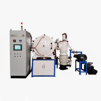
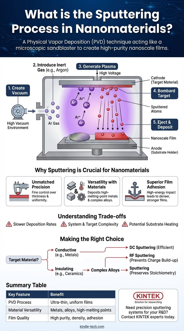
In essence, sputtering is a physical vapor deposition (PVD) process used to create extremely thin films of a material, often on the scale of nanometers. It functions like a microscopic sandblaster, where energetic ions of an inert gas bombard a source material (the "target"), physically knocking off its atoms. These dislodged atoms then travel through a vacuum and condense onto a nearby object (the "substrate"), gradually building a uniform coating.
The critical insight is that sputtering is not a chemical reaction or a melting process. It is a purely mechanical, momentum-transfer phenomenon that uses energized plasma in a vacuum to precisely control the deposition of high-purity films, making it indispensable for fabricating advanced nanomaterials and electronic components.
The Anatomy of the Sputtering Process
Sputtering is a highly controlled, multi-stage process that takes place inside a sealed vacuum chamber. Each step is critical to achieving a high-quality, uniform nanoscale film.
Step 1: Creating the Vacuum Environment
Before the process begins, the chamber is pumped down to a very low pressure, creating a high vacuum.
This initial step is crucial for removing air, moisture, and other residual gases. Any contaminants would interfere with the process and compromise the purity of the resulting film.
Step 2: Introducing the Inert Gas
Once a sufficient vacuum is achieved, a pure, inert gas—most commonly Argon (Ar)—is introduced into the chamber.
Argon is used because it is chemically non-reactive and has a suitable atomic mass. It will not form compounds with the target material, ensuring the deposited film maintains its original composition.
Step 3: Generating the Plasma
A high voltage is applied within the chamber, energizing the argon gas and stripping electrons from the argon atoms.
This creates a plasma, which is a highly ionized state of matter consisting of positive argon ions (Ar+) and free electrons. This glowing discharge is the source of the energetic ions needed for sputtering.
Step 4: Bombarding the Target
The target, which is the source material to be deposited, is given a negative electrical charge, turning it into a cathode.
The positively charged argon ions in the plasma are naturally attracted to the negatively charged target. They accelerate towards it, colliding with its surface with significant kinetic energy.
Step 5: Ejecting and Depositing Atoms
The impact from the high-energy argon ions is powerful enough to knock atoms loose from the target material's surface. This ejection of atoms is the "sputtering" effect.
These sputtered atoms travel in a straight line through the low-pressure environment until they strike the substrate, which is strategically placed to intercept them. They condense on the substrate's surface, building up a thin film one atomic layer at a time.
Why Sputtering is Crucial for Nanomaterials
While other methods exist, sputtering offers unique advantages that make it a cornerstone technology in nanotechnology and semiconductor manufacturing.
Unmatched Precision and Uniformity
The process allows for exceptionally fine control over the thickness and uniformity of the film, which is essential when working at the nanoscale. It can create smooth, dense films with consistent properties across a large surface area.
Versatility with Materials
Sputtering is particularly effective for depositing materials with very high melting points, such as refractory metals, which are difficult or impossible to deposit using thermal evaporation methods. It also excels at depositing complex alloys and compounds while preserving their original chemical ratio.
Superior Film Adhesion
The sputtered atoms arrive at the substrate with considerable energy. This higher impact energy generally results in a denser film with stronger adhesion to the substrate surface compared to lower-energy deposition techniques.
Understanding the Trade-offs
Despite its advantages, sputtering is a complex process with inherent limitations that must be considered.
Slower Deposition Rates
Compared to some other methods like thermal evaporation, sputtering can be a relatively slow process. This can impact manufacturing throughput for applications requiring very thick films.
System and Target Complexity
Sputtering systems are sophisticated and require significant capital investment for vacuum pumps, power supplies, and process controllers. The targets themselves can also be expensive to manufacture.
Potential for Substrate Heating
The continuous bombardment of energetic particles can lead to significant heating of the substrate. For temperature-sensitive materials, this requires implementing cooling systems to prevent damage.
Making the Right Choice for Your Material
The specific type of sputtering process you use is determined by the electrical properties of your target material.
- If your primary focus is depositing conductive materials (e.g., metals): Standard Direct Current (DC) sputtering is the most efficient and widely used method.
- If your primary focus is depositing insulating materials (e.g., ceramics, oxides): Radio Frequency (RF) sputtering is required to prevent a positive charge from building up on the target surface, which would halt the process.
- If your primary focus is depositing complex alloys or compounds: Sputtering is an excellent choice, as it generally preserves the material's original stoichiometry in the final film.
Ultimately, sputtering provides a powerful and versatile tool for engineering materials at the atomic scale, enabling the fabrication of countless advanced devices.
Summary Table:
| Key Feature | Benefit for Nanomaterials |
|---|---|
| Process Type | Physical Vapor Deposition (PVD) |
| Primary Use | Creating ultra-thin, uniform films |
| Material Versatility | Excellent for metals, alloys, and high-melting-point materials |
| Film Quality | High purity, density, and strong adhesion |
| Common Applications | Semiconductors, nanotechnology, optical coatings |
Need to deposit a high-purity, uniform nanoscale film?
KINTEK specializes in precision lab equipment, including sputtering systems, to meet the exacting demands of materials science and nanotechnology R&D. Our expertise helps you achieve superior film quality and consistency for your most critical projects.
Contact our experts today to discuss how our solutions can advance your research and development.
Visual Guide
Related Products
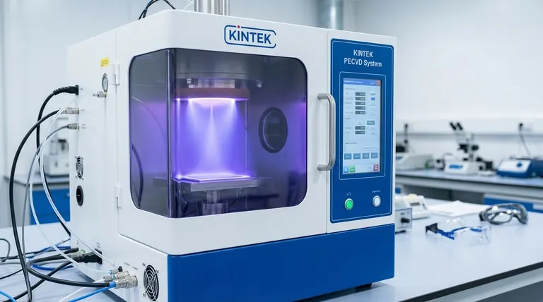
- RF PECVD System Radio Frequency Plasma-Enhanced Chemical Vapor Deposition RF PECVD
- Chemical Vapor Deposition CVD Equipment System Chamber Slide PECVD Tube Furnace with Liquid Gasifier PECVD Machine
- Split Chamber CVD Tube Furnace with Vacuum Station Chemical Vapor Deposition System Equipment Machine
- VHP Sterilization Equipment Hydrogen Peroxide H2O2 Space Sterilizer
- 1200℃ Controlled Atmosphere Furnace Nitrogen Inert Atmosphere Furnace
People Also Ask
- What is an example of PECVD? RF-PECVD for High-Quality Thin Film Deposition
- How does RF power create plasma? Achieve Stable, High-Density Plasma for Your Applications
- What are the applications of PECVD? Essential for Semiconductors, MEMS, and Solar Cells
- What is the principle of plasma enhanced chemical vapor deposition? Achieve Low-Temperature Thin Film Deposition
- How are PECVD and CVD different? A Guide to Choosing the Right Thin-Film Deposition Process