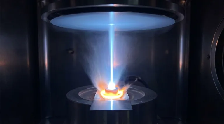
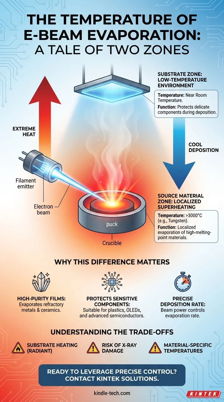
In e-beam evaporation, there is no single operating temperature. Instead, the process creates two distinct and critical temperature zones: an extremely hot, localized spot on the source material that causes evaporation, and a much cooler substrate where the material is deposited. The source material can be heated to well over 3000°C, while the substrate can remain near room temperature.
The core concept to grasp is that the "temperature" of e-beam evaporation is not one number but a tale of two environments. The technique's primary advantage lies in its ability to create a massive temperature gradient between a superheated source and a cool substrate, enabling the deposition of high-melting-point materials onto sensitive surfaces.
The Two Critical Temperature Zones
To understand the process, you must differentiate between the temperature of the material being evaporated and the temperature of the surface receiving the new film.
The Source Material: Localized Superheating
The electron beam is a highly focused stream of energy. It strikes a very small area on the surface of the source material (the "puck" or "ingot") in a crucible.
This intense, localized energy input heats that small spot to its boiling point, causing atoms to sublimate or evaporate into the vacuum chamber. This temperature is entirely dependent on the material being deposited and can be extreme, such as over 3400°C for tungsten.
The Substrate: A Low-Temperature Environment
Simultaneously, the substrate (the wafer or component being coated) is positioned at a distance from the source. Because the heating is so localized and the process occurs in a high vacuum, very little heat is transferred to the substrate.
This is the key advantage of the technique. The substrate temperature remains low, often close to room temperature, preventing damage to delicate components like plastics or pre-existing integrated circuits. The reference to "low substrate temperatures" highlights this specific benefit.
Why This Temperature Difference Matters
The ability to separate the source and substrate temperatures gives e-beam evaporation its unique capabilities and precision.
Enabling High-Purity Films
The extremely high temperatures achievable at the source allow for the evaporation of materials with very high melting points, such as refractory metals (tungsten, tantalum) and ceramics (titanium dioxide). This is difficult or impossible with other methods like standard thermal evaporation.
Protecting Sensitive Components
Because the substrate remains cool, you can deposit conductive or optical films onto materials that would be damaged by high heat. This is critical for applications in organic electronics (OLEDs), medical devices, and advanced semiconductor manufacturing.
Controlling Deposition Rate
The temperature of the source spot, which is controlled by the electron beam's power, directly influences the evaporation rate. A higher beam power creates a hotter spot, which releases more vapor, resulting in a faster deposition rate on the substrate. This provides a precise lever for controlling film thickness.
Understanding the Trade-offs
While powerful, the temperature dynamics of e-beam evaporation are not without complexities that require management.
Substrate Heating Is Not Zero
Although the substrate stays relatively cool, it is not perfectly isolated. It will experience some radiant heating from the molten source material, especially during long deposition runs. For high-precision applications, active substrate cooling is often necessary to maintain temperature stability.
Risk of X-ray Damage
When the high-energy electron beam strikes the source material, it generates X-rays as a byproduct. These X-rays can penetrate the substrate and potentially damage sensitive electronic devices, which is a known consideration in semiconductor fabrication.
Material-Specific Temperatures
It is critical to remember that the required source temperature is a property of the material itself. There is no universal setting; the process must be tuned specifically for the boiling point and thermal properties of the material being deposited.
How to Think About Temperature in Your Process
Your approach should be dictated by your end goal, focusing on either the source or the substrate environment.
- If your primary focus is depositing high-melting-point materials: Your goal is to deliver enough beam power to achieve and sustain the material's evaporation temperature at the source.
- If your primary focus is protecting a delicate substrate: Your main concern is managing and often actively cooling the substrate to prevent radiant heating from affecting your component.
- If your primary focus is precise rate control: The temperature of the source, controlled by beam power, is your primary lever for adjusting the deposition rate from 0.1 to 100 nm/minute.
Ultimately, mastering e-beam evaporation means managing these distinct temperature zones to achieve your specific material and substrate goals.
Summary Table:
| Temperature Zone | Typical Range | Key Function |
|---|---|---|
| Source Material | > 3000°C (e.g., Tungsten) | Localized evaporation of high-melting-point materials |
| Substrate | Near room temperature | Protects delicate components during deposition |
Ready to leverage the precise temperature control of e-beam evaporation for your lab's thin-film applications? KINTEK specializes in advanced lab equipment and consumables, providing the tools and expertise to deposit high-purity films on even the most sensitive substrates. Whether you're working with refractory metals, ceramics, or delicate electronics, our solutions ensure optimal process management. Contact us today to discuss how we can enhance your deposition capabilities!
Visual Guide
Related Products
- Electron Beam Evaporation Coating Oxygen-Free Copper Crucible and Evaporation Boat
- Electron Beam Evaporation Coating Tungsten Crucible and Molybdenum Crucible for High Temperature Applications
- Electron Beam Evaporation Coating Gold Plating Tungsten Molybdenum Crucible for Evaporation
- Electron Beam Evaporation Coating Conductive Boron Nitride Crucible BN Crucible
- E Beam Crucibles Electron Gun Beam Crucible for Evaporation
People Also Ask
- What is the voltage of e-beam evaporation? Achieve Precise Thin-Film Deposition
- How is an electron beam evaporator cooled during deposition? Essential Thermal Management for Stable Processes
- What is the container that holds the metal source material called in e-beam evaporation? Ensure Purity and Quality in Your Thin-Film Deposition
- What are the applications of electron beams? From Nanoscale Imaging to Industrial Manufacturing
- What are the applications of e-beam evaporation? Achieve High-Purity Coatings for Optics & Electronics


