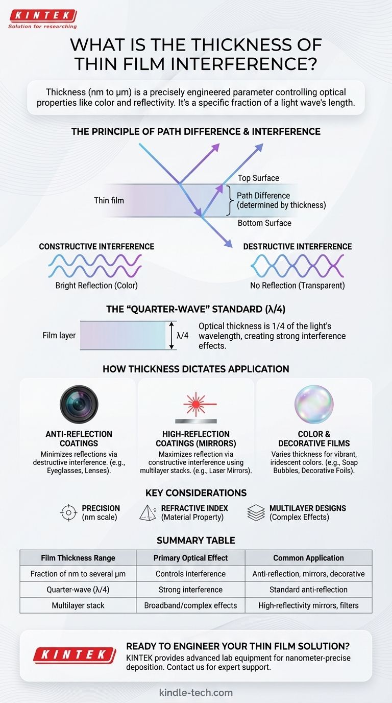
The thickness of a thin film used for interference effects typically ranges from fractions of a nanometer up to several micrometers. This thickness is not an arbitrary dimension but a highly engineered parameter directly responsible for the film's optical properties, such as its color or reflectivity.
The essential takeaway is that a thin film's thickness is deliberately chosen to be a specific fraction of a light wave's length. This precise control allows engineers to manipulate how light waves interact, determining which colors are reflected and which are transmitted.
The Fundamental Role of Thickness in Interference
The phenomenon of thin-film interference arises from the interaction of light waves reflecting from the top and bottom surfaces of the film. The film's thickness is the most critical factor governing this interaction.
The Principle of Path Difference
When light hits a thin film, some of it reflects off the top surface. The rest of the light enters the film, travels through it, and reflects off the bottom surface before traveling back up and exiting.
The light wave reflecting from the bottom travels a longer path than the one reflecting from the top. This extra distance is known as the path difference, and it is directly determined by the film's thickness.
Constructive vs. Destructive Interference
The relationship between the waves exiting the film dictates the visual effect.
If the path difference causes the two reflecting waves to align perfectly (in-phase), they reinforce each other. This is constructive interference, which produces a bright reflection of a specific color.
If the path difference causes the waves to be perfectly misaligned (out-of-phase), they cancel each other out. This is destructive interference, which eliminates the reflection.
The "Quarter-Wave" Standard
A common and highly effective design is the quarter-wave film, where the film's optical thickness is equal to one-quarter of the light's wavelength.
This specific thickness forces the light reflecting from the bottom to travel an extra half-wavelength (down and back up). This precise shift is ideal for creating strong constructive or destructive interference, depending on the materials used.
How Thickness Dictates Application
By precisely controlling the film's thickness, we can engineer a wide variety of optical components.
Anti-Reflection Coatings
For camera lenses or eyeglasses, the goal is to minimize reflections. A single-layer coating is designed with a thickness that causes destructive interference for visible light, primarily in the green-yellow spectrum where our eyes are most sensitive. This effectively cancels out the reflection, allowing more light to pass through.
High-Reflection Coatings (Mirrors)
To create a highly reflective mirror, such as those used in lasers, multiple layers of thin films are stacked. By alternating materials and carefully controlling the thickness of each layer, engineers can create constructive interference across a very broad range of wavelengths, reflecting nearly 100% of the incoming light.
Color and Decorative Films
The iridescent colors seen on soap bubbles, oil slicks, or the back of a beetle are natural examples of thin-film interference. The thickness of the film varies, causing different colors (wavelengths) to be constructively reflected at different points, creating a shimmering rainbow effect.
Understanding the Trade-offs
While the concept is straightforward, practical application involves important considerations.
Precision vs. Cost
Achieving a uniform thickness at the nanometer scale requires sophisticated and expensive deposition equipment, such as sputtering or vapor deposition systems. Thicker, less precise films are generally easier and cheaper to produce but offer less control over optical properties.
The Role of Refractive Index
Thickness is only half of the equation. The material's refractive index also dictates how much the light slows down inside the film, which directly affects the optical path difference. A correct calculation must account for both the physical thickness and the refractive index of the material.
Single vs. Multilayer Designs
A single-layer film can only be optimized for a single wavelength or a narrow band of light. To achieve complex effects, like a mirror that reflects a wide band of colors or a filter that blocks specific laser lines, a multilayer stack is necessary. This adds significant design and manufacturing complexity.
Making the Right Choice for Your Goal
The ideal thickness is entirely dependent on the desired optical outcome.
- If your primary focus is anti-reflection: You need a film precisely engineered to a quarter-wavelength of the target light, factoring in the material's refractive index to cause destructive interference.
- If your primary focus is creating specific colors: The thickness must be tuned to constructively interfere with the desired visible wavelengths, leading to a vibrant reflection of that color.
- If your primary focus is a high-efficiency mirror: You will need a complex multilayer stack of alternating materials and thicknesses designed to create broad constructive interference.
Ultimately, thickness is the primary lever used to tune a film's performance to a specific optical requirement.
Summary Table:
| Film Thickness Range | Primary Optical Effect | Common Application |
|---|---|---|
| Fraction of nm to several µm | Controls constructive/destructive interference | Anti-reflection coatings, mirrors, decorative films |
| Quarter-wave (λ/4) thickness | Strong interference for target wavelength | Standard for single-layer anti-reflection coatings |
| Multilayer stack | Broadband or complex optical effects | High-reflectivity mirrors, precision optical filters |
Ready to Engineer Your Thin Film Solution?
The precise thickness of your thin film is the key to unlocking its optical potential. At KINTEK, we specialize in providing the advanced lab equipment and expert support needed to deposit and control thin films with nanometer accuracy. Whether you're developing anti-reflective coatings, high-efficiency mirrors, or specialized decorative films, our solutions help you achieve the exact interference effects you require.
Contact us today to discuss your project and discover how KINTEK's expertise in lab equipment can bring clarity and precision to your thin film applications.
Visual Guide
Related Products
People Also Ask
- What are the general operating procedures for a thin-layer spectroelectrochemical cell during an experiment? Master Synchronized Data Collection
- What operational environments and sealing options are available for the thin-layer spectroelectrochemical cell?
- What are the recommended post-experiment procedures for cleaning and storing the thin-layer spectroelectrochemical cell?
- What are the construction materials and design features of the thin-layer spectroelectrochemical cell body? Explored
- What precautions should be taken regarding voltage and polarity when using the thin-layer spectroelectrochemical cell?
