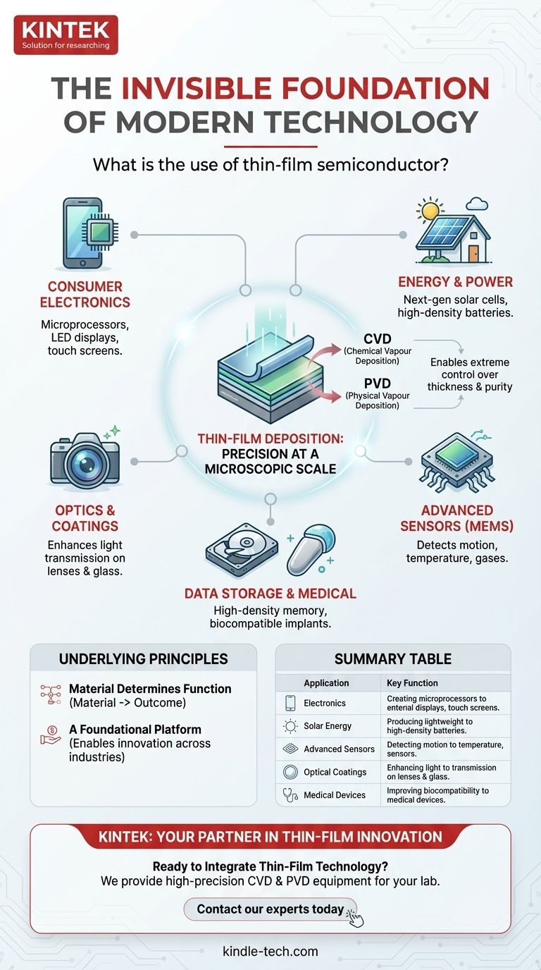
Thin-film semiconductors are the invisible foundation of modern technology. They are ultra-thin layers of material used in everything from the microprocessors in your laptop and the screen on your phone to solar panels and advanced medical sensors. Their primary use is to create microscopic electronic circuits and specialized coatings that precisely control electricity, light, and data.
The true significance of thin-film semiconductors isn't just one application, but the underlying manufacturing process—thin-film deposition—which gives engineers precise control to build the complex, microscopic structures that power our digital world.
The Core Function: Precision at a Microscopic Scale
The power of thin-film technology comes from the ability to deposit materials one atomic layer at a time. This unlocks capabilities that are impossible with bulk materials.
Controlling Electrical Current
At their core, thin-film semiconductors are used to build the fundamental components of all electronics. They form the transistor arrays that act as microscopic on-off switches inside every integrated circuit and microprocessor.
This precise control over conductivity allows for the creation of incredibly dense and powerful micro-circuitry, which is the brain of any modern electronic device.
The Enabling Manufacturing Process
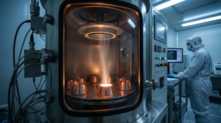
These films are created using methods like Chemical Vapour Deposition (CVD) and Physical Vapour Deposition (PVD). These processes allow for extreme precision in controlling a film's thickness, composition, and purity.
CVD is the dominant method in the semiconductor industry for its high accuracy, while PVD is highly versatile for creating specialized coatings and high-purity films.
More Than Just Circuits
While semiconductors are a primary application, the thin-film deposition process can be used with many materials. This allows engineers to create layers with specific optical, magnetic, or physical properties.
Key Applications Across Industries
Because thin-film deposition is a foundational manufacturing technique, its applications are incredibly diverse, touching nearly every aspect of modern life.
Consumer Electronics
This is the most common and visible application. Thin films are critical for producing the components in mobile phones, laptops, and tablets. They are used to create both the processing chips and the vibrant LED displays and responsive touch screens.
Energy and Power
Thin-film technology is essential for creating next-generation solar cells, which can be integrated into materials like rooftop tiles. It is also used in the development of advanced, high-density batteries.
Optics and Coatings
The same deposition process is used to apply optical coatings to lenses and glass. These ultra-thin layers improve the transmission, reflection, and refraction of light, leading to better cameras, eyeglasses, and mirrors.
Advanced Sensors (MEMS)
Micro-Electro-Mechanical Systems, or MEMS, are microscopic devices that often rely on thin films. These are used as highly sensitive sensors to detect everything from smoke and radon to changes in temperature, movement, and altitude.
Data Storage and Medical Devices
Thin magnetic films are used to create high-density computer memory. In the medical field, specialized thin-film coatings are applied to medical implants to improve biocompatibility and performance.
The Underlying Principles
Understanding thin-film technology requires looking beyond a single use case and focusing on the core principles that make it so versatile.
Material Determines Function
The term "thin-film semiconductor" refers to a specific application where a semiconducting material (like silicon) is deposited. However, the function of the film is entirely dependent on the material used.
Depositing a magnetic material creates data storage. Depositing a light-emitting compound creates an LED. The deposition process is the tool; the material choice defines the outcome.
A Foundational Technology, Not a Single Product
It is more accurate to think of thin-film deposition as a platform technology rather than a single component. It is a fundamental manufacturing capability that enables miniaturization and enhanced material properties across countless industries.
The ability to build devices atom by atom is what has driven the incredible pace of technological advancement over the past several decades.
How This Technology Shapes Your Goal
Understanding the role of thin films clarifies how modern devices are engineered.
- If your primary focus is on computing power: Know that thin films are what enable the billions of transistors packed into a modern microprocessor.
- If your primary focus is on renewable energy: Recognize that thin-film technology is key to creating efficient, lightweight, and versatile solar cells.
- If your primary focus is on device displays: Understand that thin films control the light-emitting pixels that create vibrant, high-resolution screens.
- If your primary focus is on advanced manufacturing: Appreciate that thin-film deposition is the core process enabling miniaturization and material innovation across all high-tech fields.
Ultimately, thin-film technology is a masterclass in material science, allowing us to engineer the properties of our world at a near-atomic level.
Summary Table:
| Application | Key Function | Common Materials/Processes |
|---|---|---|
| Consumer Electronics | Creating microprocessors and LED displays | Silicon, CVD/PVD Deposition |
| Solar Energy | Producing lightweight, efficient solar cells | Cadmium Telluride, CIGS |
| Advanced Sensors (MEMS) | Detecting motion, temperature, and gases | Polycrystalline Silicon |
| Optical Coatings | Enhancing light transmission on lenses | Various Oxides, PVD |
| Medical Devices | Improving biocompatibility of implants | Titanium Nitride, Diamond-like Carbon |
Ready to Integrate Thin-Film Technology into Your Lab?
At KINTEK, we specialize in providing the high-precision lab equipment and consumables needed for advanced thin-film deposition processes like CVD and PVD. Whether you're developing next-generation semiconductors, solar cells, or MEMS sensors, our solutions ensure the material purity and process control required for success.
Let's discuss how we can support your innovation: Contact our experts today to explore the right equipment for your specific application.
Visual Guide
Related Products
- Customizable PTFE Wafer Carriers for Semiconductor and Lab Applications
- Custom PTFE Wafer Holders for Lab and Semiconductor Processing
- Thin-Layer Spectral Electrolysis Electrochemical Cell
- Aluminum-Plastic Flexible Packaging Film for Lithium Battery Packaging
People Also Ask
- Is PTFE corrosion resistant? Discover the Ultimate Chemical Resistance for Your Lab
- What is the function of a customized PTFE cap in IL-TEM? Bridge the Gap Between Microscopy and Electrochemistry
- What are the technical advantages of using PTFE laboratory consumables? Ensure Ultimate Chemical Resistance
- How is PTFE utilized for insulation in Alloy 22 corrosion setups? Ensure Signal Purity & Accuracy
- Why is slender PTFE tubing necessary for flow control in multi-channel catalyst aging? Ensure Equal Gas Distribution