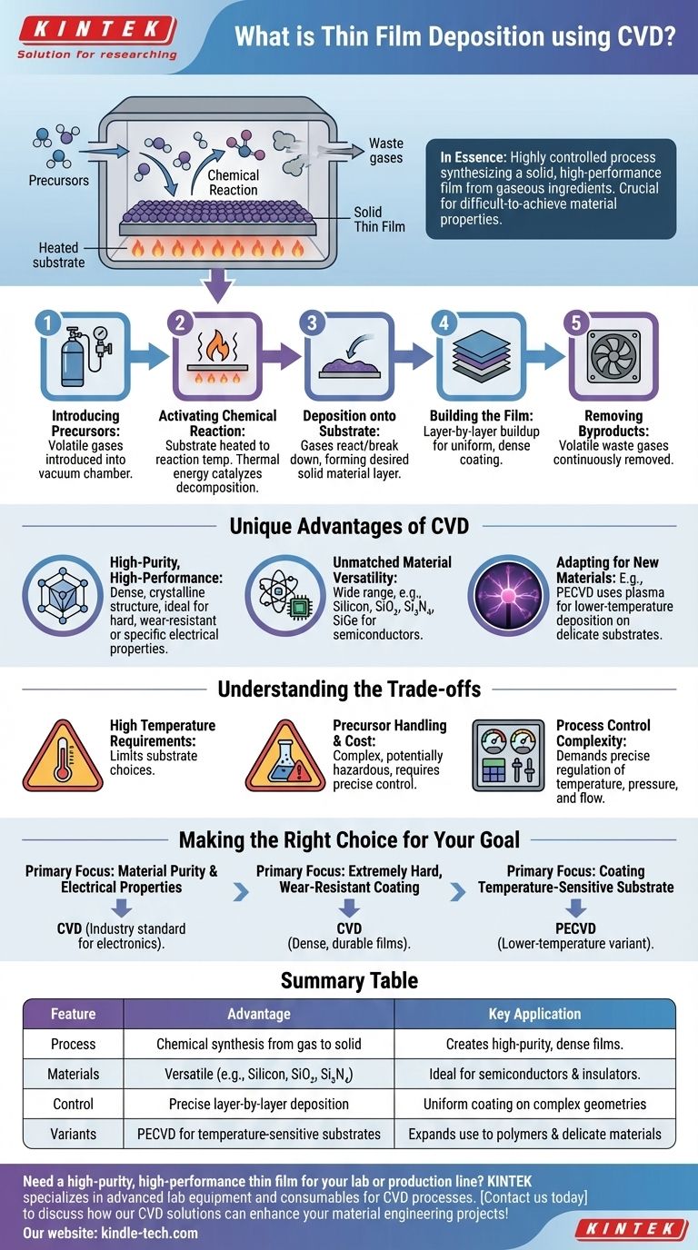
In essence, Chemical Vapor Deposition (CVD) is a highly controlled manufacturing process used to build a solid, high-performance thin film on a surface from gaseous ingredients. It relies on inducing chemical reactions with volatile precursor gases that decompose and bond onto a substrate, effectively constructing the desired material one layer at a time. This method is crucial for creating materials with specific properties that are difficult, if not impossible, to achieve with other techniques.
The core principle of CVD is not merely coating a surface, but rather synthesizing a new solid material directly onto it. By controlling the chemical reactions of gases, CVD allows for the creation of exceptionally pure, dense, and high-performance thin films essential for advanced electronics and materials science.
How CVD Fundamentally Works
The CVD process is a carefully orchestrated sequence of events that transforms gas into a solid film. Each step requires precise control to achieve the desired outcome.
Step 1: Introducing the Precursors
The process begins by introducing one or more volatile precursor gases into a reaction chamber, which usually operates under a vacuum. These precursors contain the chemical elements required for the final film.
Step 2: Activating the Chemical Reaction
The substrate within the chamber is heated to a specific reaction temperature. This thermal energy provides the catalyst for the precursor gases to react with each other or to decompose.
Step 3: Deposition onto the Substrate
As the gases react or break down on the hot substrate surface, the desired solid material is formed. This new material bonds to the surface, beginning the formation of a thin, solid layer.
Step 4: Building the Film
Over time, this deposition process continues, building up the coating layer by layer. This allows for the creation of a uniform, dense film that covers all exposed areas of the part.
Step 5: Removing the Byproducts
The chemical reactions almost always create volatile byproducts. These unwanted gases are continuously removed from the chamber by a steady gas flow, which is critical for maintaining the purity of the depositing film.
The Unique Advantages of CVD
Engineers and scientists choose CVD when the properties of the final film are paramount. The nature of the process enables a level of quality and versatility that other methods struggle to match.
Creating High-Purity, High-Performance Films
Because the film is built from a chemical reaction, it's possible to achieve an exceptionally high degree of purity and a dense, crystalline structure. This makes CVD ideal for depositing very hard, wear-resistant coatings or materials with specific electrical properties.
Unmatched Material Versatility
A vast range of materials can be deposited using CVD. This is particularly important in the semiconductor industry for creating technologically critical insulators and semiconductors.
Examples include:
- Polysilicon, Amorphous Silicon, and Epitaxial Silicon
- Silicon Dioxide (SiO₂)
- Silicon Nitride (Si₃N₄)
- Silicon-Germanium (SiGe)
Adapting the Process for New Materials
The core CVD concept can be modified to suit different needs. For example, Plasma-Enhanced CVD (PECVD) uses plasma instead of just high heat to drive the reaction. This lower-temperature variation allows for the deposition of materials, including organic polymers, onto substrates that cannot withstand high heat.
Understanding the Trade-offs
While powerful, CVD is not a universal solution. Understanding its inherent challenges is key to using it effectively.
High Temperature Requirements
Traditional thermal CVD often requires very high temperatures to initiate the necessary chemical reactions. This can limit the types of substrate materials that can be used without being damaged.
Precursor Handling and Cost
The precursor gases can be complex, expensive, and sometimes hazardous. The chemistry must be perfectly understood and controlled to produce the desired film without unwanted impurities.
Process Control Complexity
Achieving a uniform, high-quality film demands precise control over temperature, pressure, and gas flow rates throughout the chamber. The equipment needed to maintain this level of control can be sophisticated and costly.
Making the Right Choice for Your Goal
Selecting the right deposition technique depends entirely on your project's end goal.
- If your primary focus is material purity and electrical properties: CVD is the industry standard for creating the high-performance semiconductor and insulator films that power modern electronics.
- If your primary focus is creating an extremely hard, wear-resistant coating: CVD excels at producing dense, durable films that can significantly extend the life of tools and components.
- If your primary focus is coating a temperature-sensitive substrate: You should investigate lower-temperature variants like Plasma-Enhanced CVD (PECVD) to avoid damaging your material.
Ultimately, CVD provides an unparalleled ability to engineer materials from the molecular level up, making it a cornerstone of modern technology.
Summary Table:
| Feature | Advantage | Key Application |
|---|---|---|
| Process | Chemical synthesis from gas to solid | Creates high-purity, dense films |
| Materials | Versatile (e.g., Silicon, SiO₂, Si₃N₄) | Ideal for semiconductors & insulators |
| Control | Precise layer-by-layer deposition | Uniform coating on complex geometries |
| Variants | PECVD for temperature-sensitive substrates | Expands use to polymers & delicate materials |
Need a high-purity, high-performance thin film for your lab or production line? KINTEK specializes in advanced lab equipment and consumables for CVD processes, serving laboratories and industries that demand precision and reliability. Whether you're developing next-generation semiconductors or require durable, wear-resistant coatings, our expertise ensures you achieve optimal results. Contact us today to discuss how our CVD solutions can enhance your material engineering projects!
Visual Guide
Related Products
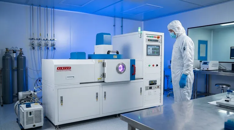
- Chemical Vapor Deposition CVD Equipment System Chamber Slide PECVD Tube Furnace with Liquid Gasifier PECVD Machine
- Customer Made Versatile CVD Tube Furnace Chemical Vapor Deposition Chamber System Equipment
- HFCVD Machine System Equipment for Drawing Die Nano-Diamond Coating
- Split Chamber CVD Tube Furnace with Vacuum Station Chemical Vapor Deposition System Equipment Machine
- Multi Heating Zones CVD Tube Furnace Machine Chemical Vapor Deposition Chamber System Equipment
People Also Ask
- What is plasma enhanced chemical vapor deposition PECVD equipment? A Guide to Low-Temperature Thin Film Deposition
- Why is Chemical Vapor Deposition (CVD) equipment uniquely suited for constructing hierarchical superhydrophobic structures?
- What is the chemical vapor deposition growth process? Build Superior Thin Films from the Atom Up
- How are carbon nanotubes grown? Master Scalable Production with Chemical Vapor Deposition
- What types of substrates are used in CVD to facilitate graphene films? Optimize Graphene Growth with the Right Catalyst


