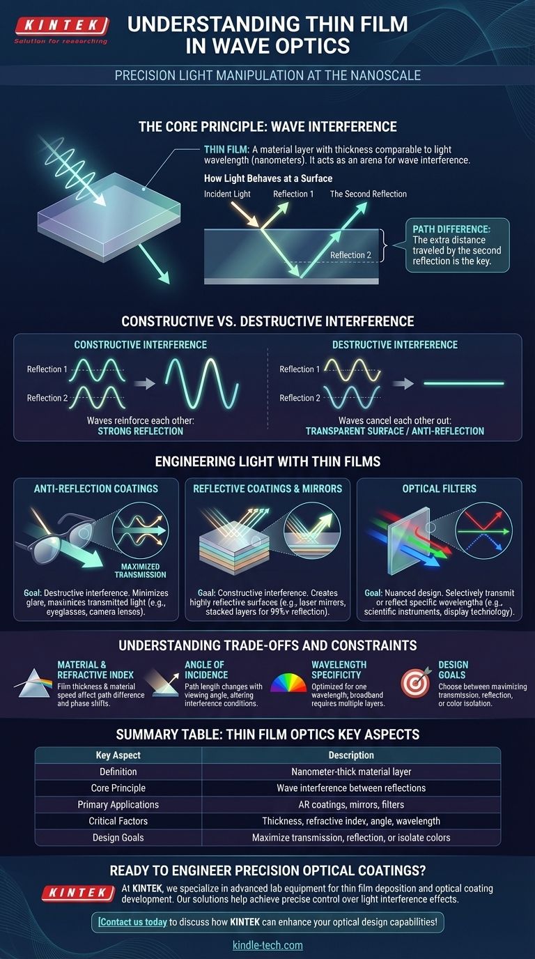
In wave optics, a thin film is a layer of material so thin that its thickness is comparable to the wavelength of light itself, typically measured in nanometers. This precise thickness is not an incidental property; it is the core mechanism that allows the film to manipulate light. By forcing light waves reflecting from its top and bottom surfaces to interact, a thin film uses the principle of interference to control which wavelengths are reflected and which are transmitted.
The essential insight is that a thin film acts as an arena for wave interference. By precisely engineering its thickness and refractive index, we can dictate whether reflecting light waves reinforce each other to create a strong reflection or cancel each other out to create a transparent surface.
The Core Principle: Wave Interference
To understand thin films, one must first understand how they manipulate light waves. The entire effect is built upon the principle of interference, which occurs when two or more waves overlap.
How Light Behaves at a Surface
When a light wave strikes the top surface of a thin film, a portion of it reflects immediately. The rest of the wave is transmitted, passing into the film.
The Second Reflection
The light wave that entered the film travels through it until it reaches the bottom surface. At this boundary, another portion of the wave reflects back up, eventually exiting through the top surface.
The Critical Path Difference
You now have two separate reflected waves traveling in the same direction: one from the top surface and one from the bottom. The wave that reflected from the bottom surface traveled a longer path. This path difference is the key to the entire phenomenon.
Constructive vs. Destructive Interference
If the extra distance traveled by the second wave causes its peaks and troughs to align perfectly with the first wave, they combine to create a stronger, brighter reflection. This is constructive interference.
If that extra distance causes the peaks of the second wave to align with the troughs of the first, they cancel each other out, resulting in little or no reflection. This is destructive interference.
Engineering Light with Thin Films
By precisely controlling a film's thickness, engineers can pre-determine the path difference for specific wavelengths (colors) of light, forcing either constructive or destructive interference.
Creating Anti-Reflection Coatings
The most common application is an anti-reflection coating, seen on eyeglasses and camera lenses. The film's thickness is chosen so that for visible light, the reflected waves are perfectly out of sync, causing them to cancel each other out. This minimizes glare and maximizes the amount of light transmitted through the lens.
Designing Reflective Coatings and Mirrors
Conversely, a thin film can be engineered to create a highly reflective surface. By choosing a thickness that causes reflected waves to be perfectly in sync, they combine to produce a reflection much stronger than the base material would alone. Stacking multiple layers can create mirrors that reflect over 99% of specific light colors.
Building Optical Filters
Thin films are also used as optical filters that selectively transmit some wavelengths while reflecting others. A film might be designed to cause constructive interference for red light (reflecting it) while allowing blue and green light to pass through. This is the technology behind many specialized optical instruments and filters.
Understanding the Trade-offs and Constraints
While powerful, thin film effects are governed by precise physical constraints that are critical to understand in any practical application.
Material and Refractive Index
The film's thickness is only half the equation. The refractive index of the material determines how much the light slows down inside the film, which directly affects the path difference. It also determines if a phase shift occurs upon reflection, which can flip a wave and must be accounted for in the design.
Angle of Incidence Dependency
Most thin film coatings are optimized for light hitting the surface at a perpendicular angle (0 degrees). If you view the surface from a sharp angle, the path the light takes through the film becomes longer. This changes the interference conditions, which is why some coated lenses show colored sheens when viewed from the side.
Wavelength Specificity
A coating designed for one wavelength will not be perfectly efficient for others. An anti-reflection coating optimized for the center of the visible spectrum (green light) will be less effective for deep red or violet light. This is why high-end optics use multiple layers of different films to achieve broadband performance.
Making the Right Choice for Your Goal
The application of thin film principles depends entirely on the desired optical outcome. Your design choice is a direct function of the interference effect you need to produce.
- If your primary focus is maximizing light transmission (e.g., camera lenses, solar cells): Your goal is to engineer destructive interference to create a highly effective anti-reflection coating.
- If your primary focus is maximizing reflection (e.g., laser mirrors, specialized optics): Your goal is to engineer constructive interference, often with multiple layers, to build a highly reflective dielectric mirror.
- If your primary focus is isolating specific colors (e.g., scientific filters, display technology): Your goal is a nuanced design that selectively creates constructive interference for wavelengths you want to reflect and destructive interference for those you want to transmit.
Ultimately, thin film optics provides a precise method for engineering the flow of light at a fundamental level.
Summary Table:
| Key Aspect | Description |
|---|---|
| Definition | Material layer with thickness comparable to light wavelength (nanometers) |
| Core Principle | Wave interference between reflections from top and bottom surfaces |
| Primary Applications | Anti-reflection coatings, reflective mirrors, optical filters |
| Critical Factors | Thickness, refractive index, angle of incidence, wavelength specificity |
| Design Goals | Maximize transmission, maximize reflection, or isolate specific colors |
Ready to engineer precision optical coatings for your application?
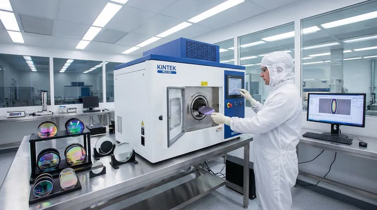
At KINTEK, we specialize in advanced lab equipment and consumables for thin film deposition and optical coating development. Our solutions help researchers and engineers achieve precise control over light interference effects for applications ranging from camera lenses to specialized optics.
Whether you need to develop anti-reflection coatings, high-reflectivity mirrors, or custom optical filters, our expertise and equipment can support your project from concept to production.
Contact us today to discuss how KINTEK's lab solutions can enhance your optical design capabilities!
Visual Guide
Related Products
- Aluminum-Plastic Flexible Packaging Film for Lithium Battery Packaging
- Thin-Layer Spectral Electrolysis Electrochemical Cell
People Also Ask
- What is organic thin film? A Guide to Engineered Molecular Layers for Advanced Tech
- How to check if a lithium battery is good? Safely Test Voltage, Capacity & Internal Resistance
- What is the thinnest coating? Unlocking Unique Properties at the Atomic Scale
- How to tell if a lithium-ion battery is bad? Spot the critical signs of failure before it's too late.
- Is there a way to test lithium batteries? Understand Voltage vs. True Health

