For RF sputter deposition, the universally accepted and most commonly used frequency is 13.56 MHz. This specific frequency is chosen not only for its physical effectiveness in the sputtering process but also because it is a globally regulated standard, preventing interference with critical communication systems.
The selection of 13.56 MHz is a deliberate engineering compromise. It balances international radio frequency regulations with the physical requirements needed to sustain a plasma and efficiently sputter non-conductive materials.
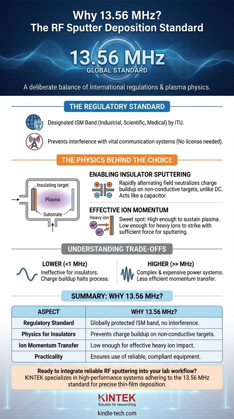
Why 13.56 MHz is the Global Standard
The choice of this exact frequency is driven primarily by regulation, which conveniently aligns with the needs of the physics involved.
The Role of ISM Bands
The International Telecommunication Union (ITU) has designated specific frequency bands for Industrial, Scientific, and Medical (ISM) purposes.
The 13.56 MHz frequency sits within one of these ISM bands. This allows equipment like RF sputtering systems to operate without requiring a special license or causing interference.
Preventing Telecommunication Interference
By operating within this protected band, RF generators used in sputtering systems are guaranteed not to disrupt vital radio, broadcast, or telecommunication services. This standardization is critical for the reliable deployment of such equipment in any lab or industrial setting worldwide.
The Physics Behind the Frequency Choice
Beyond regulation, the 13.56 MHz frequency is highly effective for the sputtering process itself, especially for insulating materials.
Enabling Sputtering of Insulators
In DC sputtering, a positive charge builds up on an insulating target, repelling the positive ions and quickly stopping the sputtering process. RF sputtering solves this.
At frequencies of 1 MHz or higher, the rapidly alternating electric field allows the insulating target to be alternately bombarded by ions and then electrons. This neutralizes the charge buildup on the target surface each cycle, enabling continuous sputtering.
Essentially, the insulating target acts like a capacitor in the RF circuit, allowing an effective current to flow and sustain the plasma.
Ensuring Effective Momentum Transfer
The 13.56 MHz frequency is also in a sweet spot for the plasma physics. It is high enough to efficiently sustain the plasma and prevent charge accumulation.
Simultaneously, it is low enough that heavy ions, such as Argon (Ar+), can still gain sufficient momentum from the electric field to strike the target with force. If the frequency were much higher, the heavy ions wouldn't be able to respond to the rapidly changing field and would have less impact energy.
Understanding the Trade-offs
While 13.56 MHz is the standard, understanding the boundaries helps clarify why it was chosen.
The Problem with Lower Frequencies
Operating below approximately 1 MHz would be ineffective for sputtering insulating materials. The alternating cycle would be too slow to prevent the target from electrically charging, which would halt the process just as it does in DC sputtering.
The Problem with Higher Frequencies
Using significantly higher frequencies (e.g., in the hundreds of MHz) would create new challenges. It would require more complex and expensive RF power delivery systems (impedance matching becomes more difficult) and could result in less efficient momentum transfer from the plasma ions to the target.
Making the Right Choice for Your Application
For nearly all users, adhering to the standard is the correct and only practical path forward.
- If your primary focus is standard thin-film deposition: Using the industry-standard 13.56 MHz is the only practical choice, as it ensures you are using compliant, reliable, and widely available equipment.
- If your primary focus is sputtering any insulating or dielectric material: RF sputtering at 13.56 MHz is essential, as DC methods will not work due to target charging.
- If your primary focus is experimental research: Deviating from 13.56 MHz would require custom-built power supplies and matching networks, along with careful shielding to avoid significant regulatory issues with radio interference.
Ultimately, the 13.56 MHz standard provides a robust and globally accepted foundation for virtually all modern RF sputtering applications.
Summary Table:
| Aspect | Why 13.56 MHz? |
|---|---|
| Regulatory Standard | Part of the globally protected ISM band, preventing interference with communications. |
| Physics for Insulators | High enough to prevent charge buildup on non-conductive targets. |
| Ion Momentum Transfer | Low enough for heavy ions (like Ar+) to respond and sputter effectively. |
| Practicality | Ensures use of reliable, widely available, and compliant equipment. |
Ready to integrate reliable RF sputtering into your lab workflow?
KINTEK specializes in high-performance lab equipment, including RF sputtering systems that adhere to the 13.56 MHz global standard. Our solutions ensure precise, consistent thin-film deposition for your research and production needs, helping you avoid regulatory issues and achieve superior results with insulating materials.
Contact us today to discuss how our sputtering technology can advance your projects.
Visual Guide
Related Products
- RF PECVD System Radio Frequency Plasma-Enhanced Chemical Vapor Deposition RF PECVD
- HFCVD Machine System Equipment for Drawing Die Nano-Diamond Coating
- 915MHz MPCVD Diamond Machine Microwave Plasma Chemical Vapor Deposition System Reactor
- Chemical Vapor Deposition CVD Equipment System Chamber Slide PECVD Tube Furnace with Liquid Gasifier PECVD Machine
- Customer Made Versatile CVD Tube Furnace Chemical Vapor Deposition Chamber System Equipment
People Also Ask
- What is an example of PECVD? RF-PECVD for High-Quality Thin Film Deposition
- How does Radio Frequency Enhanced Plasma Chemical Vapour Deposition (RF-PECVD) work? Learn the Core Principles
- How does plasma enhance CVD? Unlock Low-Temperature, High-Quality Film Deposition
- What is plasma enhanced chemical vapour deposition process? Unlock Low-Temperature, High-Quality Thin Films
- What is plasma chemical vapor deposition? A Low-Temperature Thin Film Coating Solution


