Without question, the most preferred and dominant material for manufacturing semiconductors is silicon (Si). For over half a century, silicon has served as the foundational element for the vast majority of integrated circuits, from the complex processors in your computer to the simple chips in a household appliance. Its dominance is not accidental but a result of a nearly perfect combination of electrical properties, material abundance, and manufacturing compatibility.
The core reason for silicon's supremacy isn't just its semiconductor properties; it's the unique ability to grow a stable, high-quality insulating layer of silicon dioxide (SiO₂), a feature indispensable for modern transistor fabrication.
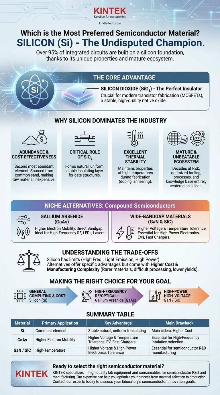
Why Silicon Dominates the Industry
Silicon's position as the industry standard is built on several key pillars that no other material has been able to match at scale.
Unmatched Abundance and Cost-Effectiveness
Silicon is the second most abundant element in the Earth's crust, right after oxygen.
It is primarily sourced from common sand (which is mostly silicon dioxide), making the raw material incredibly inexpensive and widely available. This fundamental cost advantage is a primary driver of its widespread adoption.
The Critical Role of Silicon Dioxide (SiO₂)
This is silicon's single most important advantage. When exposed to oxygen at high temperatures, silicon naturally grows a uniform, stable, and electrically insulating layer of silicon dioxide (SiO₂), also known as glass.
This native oxide is the perfect insulator needed to build the gate structure in a MOSFET (Metal-Oxide-Semiconductor Field-Effect Transistor), the fundamental building block of all modern digital electronics. No other semiconductor forms such a high-quality native oxide insulator as easily.
Excellent Thermal Stability
Silicon maintains its semiconductor properties and physical structure at the very high temperatures required during the fabrication process (doping, deposition, and annealing).
This thermal robustness allows for consistent, reliable, and high-yield manufacturing on a massive scale.
A Mature and Unbeatable Ecosystem
Decades of research, development, and trillions of dollars in investment have created a manufacturing ecosystem optimized exclusively for silicon.
The tooling, processes, and collective engineering knowledge are all centered on silicon wafers, creating an immense barrier to entry for any potential competing material.
The Niche Alternatives: Compound Semiconductors
While silicon is the workhorse for over 95% of applications, certain high-performance areas require materials with different properties. These are typically "compound semiconductors" made from two or more elements.
The Case for Gallium Arsenide (GaAs)
Gallium Arsenide has significantly higher electron mobility than silicon, meaning electrons can move through it much faster.
This property makes GaAs ideal for high-frequency applications like radio-frequency (RF) amplifiers in cell phones, radar systems, and satellite communications where speed is paramount. It also has a "direct bandgap," making it efficient at converting electricity to light for LEDs and lasers.
The Rise of Wide-Bandgap Materials (GaN & SiC)
Materials like Gallium Nitride (GaN) and Silicon Carbide (SiC) can withstand much higher voltages and temperatures than silicon.
This makes them essential for high-power electronics, such as power inverters for electric vehicles, efficient power supplies for data centers, and next-generation fast chargers.
Understanding the Trade-offs
Choosing a semiconductor material is always an exercise in balancing performance against practical limitations.
Why Silicon Isn't Always the Answer
Silicon's electron mobility limits its performance at very high radio frequencies. Its "indirect bandgap" also makes it extremely inefficient at emitting light, which is why it isn't used for LEDs or lasers. For high-power applications, it breaks down at lower voltages and temperatures than GaN or SiC.
The High Cost and Complexity of Alternatives
The primary drawback of compound semiconductors is cost and manufacturing difficulty. The raw materials are far rarer than silicon, and processing them into defect-free single crystals is a complex and expensive process.
This complexity results in smaller wafers and lower manufacturing yields, reserving these materials for applications where their specific performance advantages justify the significant extra cost.
Making the Right Choice for Your Goal
The selection of a semiconductor material is dictated entirely by the end application's performance requirements and cost constraints.
- If your primary focus is general-purpose computing and cost-effectiveness: Silicon is the only logical and undisputed choice due to its mature ecosystem and excellent all-around properties.
- If your primary focus is high-frequency radio (RF) or optical devices (LEDs): Gallium Arsenide (GaAs) is often the superior material because of its high electron mobility and efficient light-emitting properties.
- If your primary focus is high-power, high-voltage applications: Wide-bandgap materials like Gallium Nitride (GaN) or Silicon Carbide (SiC) are necessary for their thermal and electrical robustness.
Ultimately, understanding these fundamental material properties is the key to appreciating why our digital world is, and will continue to be, built on a foundation of silicon.
Summary Table:
| Material | Primary Application | Key Advantage | Main Drawback |
|---|---|---|---|
| Silicon (Si) | General Computing, Microchips | Abundant, Low Cost, Stable SiO₂ Insulator | Limited High-Frequency/High-Power Performance |
| Gallium Arsenide (GaAs) | High-Frequency RF, LEDs | High Electron Mobility, Direct Bandgap | High Cost, Complex Manufacturing |
| Gallium Nitride (GaN) / Silicon Carbide (SiC) | High-Power Electronics | High Voltage/Temperature Tolerance | Very High Cost, Manufacturing Complexity |
Ready to select the right semiconductor material for your project? The choice between silicon, GaAs, GaN, and SiC depends on your specific performance needs for computing, RF, or power applications. KINTEK specializes in providing high-quality lab equipment and consumables essential for semiconductor R&D and manufacturing. Our expertise can help you optimize your process from material selection to production.
Contact our experts today to discuss how we can support your laboratory's semiconductor innovation goals.
Visual Guide
Related Products
- Silicon Carbide (SIC) Ceramic Sheet Wear-Resistant Engineering Advanced Fine Ceramics
- Silicon Carbide (SIC) Ceramic Sheet Flat Corrugated Heat Sink for Engineering Advanced Fine Ceramics
- Silicon Carbide (SIC) Ceramic Plate for Engineering Advanced Fine Ceramics
- Precision Machined Silicon Nitride (SiN) Ceramic Sheet for Engineering Advanced Fine Ceramics
- Silicon Carbide SiC Thermal Heating Elements for Electric Furnace
People Also Ask
- What are the applications of silicon carbide? From Abrasives to High-Tech Semiconductors
- What is the process of making silicon carbide? From Raw Materials to Advanced Ceramics
- What are the properties and applications of silicon carbide ceramics? Solve Extreme Engineering Challenges
- What are the properties of SiC? Unlock High-Temperature, High-Frequency Performance
- Why is silicon carbide more efficient? Unlock Higher Power Density with SiC's Superior Material Properties