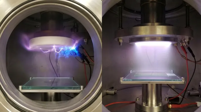
In short, DC sputtering is not used for insulating materials because the process inherently requires the target to conduct electricity, which insulators cannot do. This leads to a rapid build-up of positive charge on the target surface, effectively halting the sputtering process before it can even begin.
The core issue is electrical charge. DC sputtering relies on a constant flow of charge, but an insulating target acts as a wall, causing positive ions to accumulate and repel any further ions, stopping the deposition. The solution is to use an alternating Radio Frequency (RF) field that neutralizes this charge build-up in every cycle.

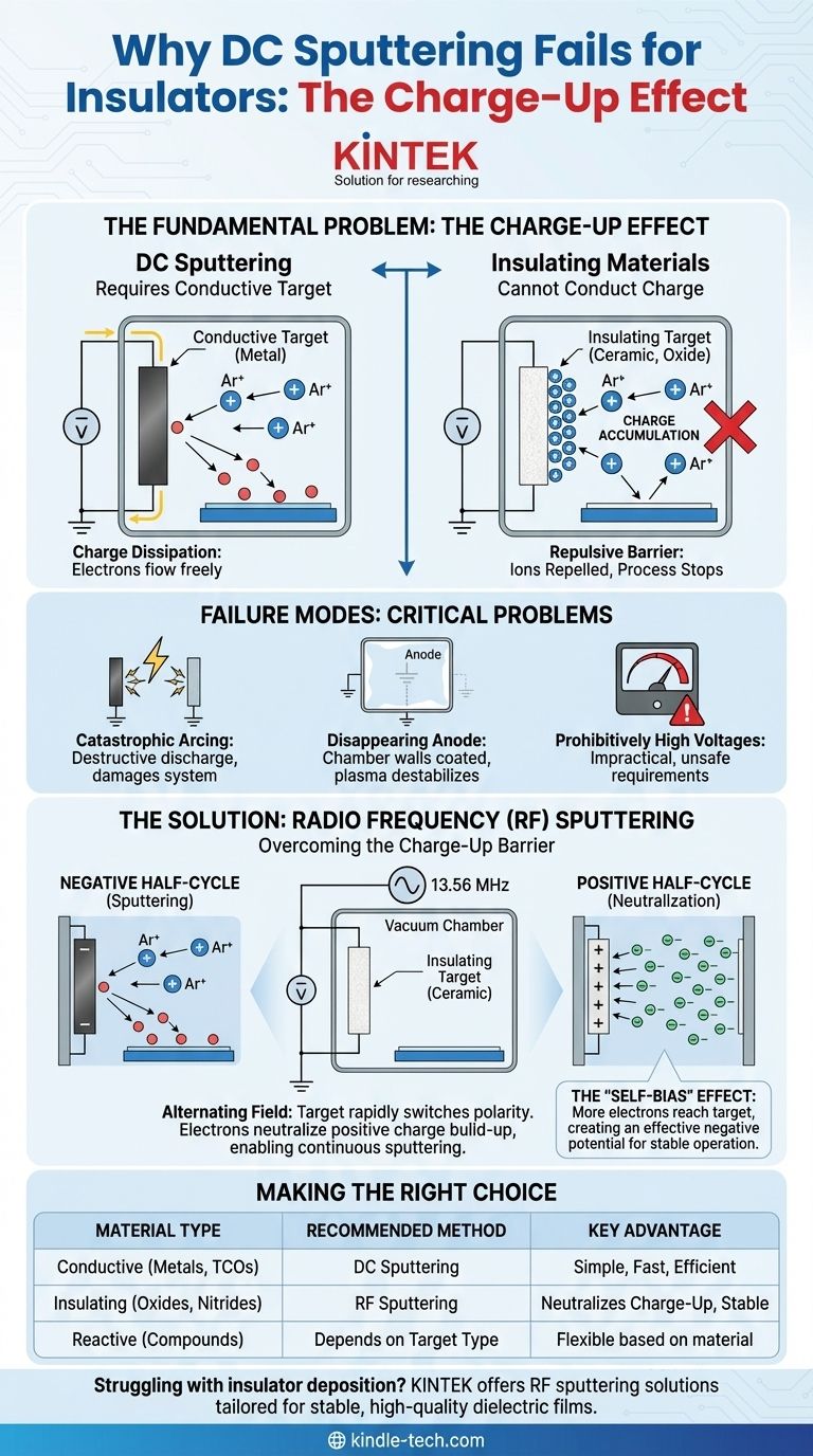
The Fundamental Problem: The Charge-Up Effect
To understand the limitation, we must first look at how the standard DC sputtering process is designed to function.
How DC Sputtering Works
In a typical DC sputtering system, a high negative DC voltage is applied to the material you want to deposit, which is called the target.
This negatively charged target is placed in a vacuum chamber filled with an inert gas, usually Argon. The high voltage ignites a plasma, stripping electrons from the Argon atoms and creating positively charged Argon ions (Ar+).
These positive ions are then accelerated by the strong negative field and slam into the target, physically knocking off, or "sputtering," atoms of the target material. These sputtered atoms then travel and deposit as a thin film on your substrate.
Why This Fails with Insulators
This entire process hinges on the target being electrically conductive. A metal target can easily dissipate the positive charge delivered by the arriving ions through the power supply connection.
An insulating target (like a ceramic oxide or nitride) cannot conduct this charge away. When the positive Argon ions strike the surface, they get stuck.
The Consequence: A Repulsive Barrier
Within microseconds, a layer of positive charge accumulates on the surface of the insulating target.
This positive surface charge creates an electric field that repels the incoming positive Argon ions from the plasma. The sputtering process quickly slows to a stop as the ions can no longer reach the target with enough energy to dislodge atoms. This phenomenon is known as the charge-up effect.
Understanding the Failure Modes
The charge-up effect isn't just inefficient; it creates several critical problems that make DC sputtering completely unviable for dielectrics.
Catastrophic Arcing
The immense potential difference between the charged-up target surface and the grounded components of the chamber can lead to uncontrolled electrical discharges.
This arcing is destructive, potentially damaging the target, the substrate, and the sputtering system itself.
The "Disappearing Anode" Effect
In a stable plasma, there must be an anode (typically the grounded chamber walls) to complete the electrical circuit.
However, as some sputtered insulating material inevitably coats the chamber walls, the anode itself becomes insulated. This further destabilizes the plasma and can extinguish it entirely.
Prohibitively High Voltages
In theory, you could try to overcome the charge-up effect by using an astronomically high voltage.
However, the required voltage would be so high that it is impractical, unsafe, and would generate more problems with arcing and heat than it would solve.
The Solution: Radio Frequency (RF) Sputtering
To overcome the charge-up barrier, a different power delivery mechanism is required: Radio Frequency (RF) sputtering.
The Alternating Field Principle
Instead of a constant negative DC voltage, RF sputtering applies a high-frequency alternating voltage (typically 13.56 MHz) to the target.
The target is rapidly switched between being negatively and positively charged, millions of times per second.
How RF Neutralizes Charge
During the half-cycle when the target is negative, it attracts positive ions, and sputtering occurs just like in the DC process.
Crucially, during the next half-cycle when the target becomes positive, it attracts a flood of highly mobile electrons from the plasma. These electrons instantly neutralize the positive charge left behind by the ions. This cleansing action prevents the charge-up effect.
The Magic of the "Self-Bias"
Because electrons are thousands of times lighter and faster than ions, the target is flooded with far more electrons during the positive cycle than ions during the negative cycle.
This imbalance creates a net negative charge on the target's surface over time. This results in an effective negative DC potential, known as the self-bias, which continuously attracts ions to maintain the sputtering process, even though the power source itself is AC.
Making the Right Choice for Your Goal
Selecting the correct sputtering technique is determined entirely by the electrical properties of your target material.
- If your primary focus is depositing conductive materials (metals, TCOs): Use DC sputtering. It is simpler, faster, more energy-efficient, and less expensive than RF sputtering.
- If your primary focus is depositing insulating materials (oxides, nitrides, ceramics): You must use RF sputtering. It is the only effective method to prevent the charge-up effect and achieve stable deposition.
- If your primary focus is reactive deposition of compounds: Both methods can be used, but your choice depends on whether the target itself is a conductor (e.g., sputtering a Ti target in a nitrogen atmosphere to get TiN) or an insulator (e.g., sputtering a SiO2 target to get a SiO2 film).
Ultimately, your success depends on matching the sputtering technique to the fundamental electrical conductivity of your source material.
Summary Table:
| Sputtering Method | Best For Materials | Key Limitation |
|---|---|---|
| DC Sputtering | Conductors (Metals, TCOs) | Fails with insulators due to charge-up effect |
| RF Sputtering | Insulators (Oxides, Nitrides, Ceramics) | Necessary to neutralize surface charge |
Struggling with thin film deposition of insulating materials? The charge-up effect can halt your DC sputtering process, but it doesn't have to stop your research. KINTEK specializes in lab equipment and consumables, providing the right RF sputtering solutions for your laboratory's unique needs. Our experts can help you select the perfect system to achieve stable, high-quality dielectric films. Contact us today to discuss how we can enhance your deposition capabilities and drive your projects forward!
Visual Guide
